The industry trend to process chips with ever-smaller chip geometries creates a greater sensitivity towards ESD-related damage which offsets the gain of a smaller package and reduced board space. The level of protection has to increase with the likelihood of user access to the chips' terminals. As CMOS products have the highest input impedance, they are likely to collect charges and are prone to damage if no additional measures are taken to absorb those violent energies. Besides the ESD event that occurs when no power is supplied to the chip, a greater hazard exists when the circuit is powered. Charge injection can lead to a possible latch-up scenario which allows high current to flow from Vcc to GND, only limited by the on resistance of the latched FETs.
Internal ESD structures, usually clamp diodes, will bypass overvoltage events to either Vcc or GND. Due to the amount of charge and the limited current-carrying capability of those structures, the charge floods the substrate with electrons and leads to a potential latch-up condition if power is applied. Due to the geometry of those ESD protection devcies, they will not be able to handle high currents for a sustained time and energy absorption is marginal. Additional external devices are required to "take the heat" and prevent an ESD-induced latch-up: the Transient Voltage Suppressor diode (TVS).
For applications that suffer from the hazard of overvoltage due to lightning, ESD potential, or accidental transient voltage streeses, a bi-directional zener diode, such as a TranZorbTM, dissipates the external energy before it gets to the silicon chip. Additional series resistors limit the maximum current that the internal structures can withstand. Outputs usually have a low impedence and require less attention. However, for maximum safety, the approach in Figure 2 requires the least board space while protecting each individual terminal.
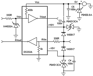
Because the RX terminal receives bipolar voltages, bi-directional TranZorbs must be used. Only for single-polarity inputs, i.e., Vcc and the TTL, use the unipolar type. This will additionally protect against polarity reversals because the unipolar TVS diode will forward-bias at 0.7V and limit the current that may flow through the reverse-biased substrate.
As lead wire inductance can create sufficient impedance to inhibit current spikes, the TVS diode may cause transient overvoltage conditions for the chip before engaging its voltage-limiting ability. Schottky diodes are of less capacitance, forward-bias at a significantly less voltage, and protect the substrate from transient supply reversal. High quality (i.e., NP0) ceramic bypass capacitors reduce the voltage increase at the supply terminals so that a single TVS diode can limit the damaging potential. Note as well that overvoltage spikes severely degrade the reliability of tantalum capacitors. Because of the high HF content of ESD discharge current, ceramic chip capacitors are valuable and need to be placed less than 1/4" away from the supply terminal. As a matter of fact, "more" is NOT better, but good HF attenuation up to the 100 MHz range, low ESR, and low inductance are desirable. Although Figure 2 shows several additional components, not all of them may be necessary to achieve a highly ESD-immune system.
Carefully evaluate which components are working best for your application and for the available real estate and budget. Because ESD-related events are sensitive to the actual parasitic capacitive and inductive discharge path, use the same setup every time. Not the actual ESD discharge voltage, but the improvement over the previous implementation counts.
The ESD-induced Latch-Up Scenario
Figure 3 depicts a simplified circuit that explains the classical latch up event. Under nominal conditions, the substrate behaves like a back-to-back zener diode: only exceeding the breakdown rating will cause a potential short between Vcc and GND.
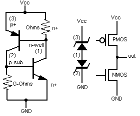
Clamp diodes are implemented into each chip to bypass overvoltage to either Vcc or GND. Due to the high voltage of charged bodies, transient discharge currents are often between 2A and 8A, causing a substantial voltage drop across the resistance between the n-well and Vcc. This resistance can vary between a few hundred milli-ohms and a few ohms, depending on the implementation of the device. As soon as this voltage drop forward-biases the p+ to n-well junction, here modeled as a PNP transistor, base current drives into the NPN section, pulling even greater current through the n+ resistance: a runaway condition. This shows the importance of having all input terminals terminated so that charges can bleed off.