Such an event would quickly discharge the battery at dangerously high currents. It has been shown that a simple zener diode, such as a 1N4736A, is sufficient protection and increases the latch-up threshold at least two-fold, and as a best case up to eight fold! This wide range of improvement depends on the actual test setup (or system), ambient conditions, and the ESD gun used for the test. Because a latch-up event is triggered through a transient peak current flowing through the substrate, a series resistor of 330 Ohms in line with Vcc makes ESD-IL a non-event. However, the additional voltage drop of up to 330mV during temperature conversion must be taken into account. In order to operate under minimum specifications, the minimum battery voltage must be above 3.9V at all times. As it is the case with all active devices, the DS243x series is no exception: power supply bypassing is recommended. Use a 1nF to 100nF ceramic capacitor for HF bypassing. Although a battery is a low-impedance voltage source, terminal inductance and lead-wire inductance can create sufficient impedance to inhibit current spikes and may cause transient overvoltage conditions for the chip.
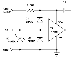
Figure 1: ESD protection devices
Most Dallas Semiconductor 1-Wire® devices can operate under "parasite" power which uses the logic high idle state of the data line to power the chip. This requires an internal diode feed an internal ~800pF capacitor for energy storage. Thus an external diode, such as D1, did not improve the ESD hardness and may be omitted.
The zener clamp diode D3 serves two purposes. First, when reverse-biased, it limits the maximum voltage between DQ and GNC. Second, when forward-biased, it clamps undershoots to -0.7V as well. Hence do not use back-to-back, or bidirectional, TranZorbsTM but uni-directional zener diodes.
High peak currents, that flow through the GND return path while an ESD event is occurring elevate the potential at the GND terminal of the chip. While the DQ data line is driven to a logic low state, this is only true for the driver (micro-controller) not for the receiver (IC). The IC's GND reference is at a higher voltage level than its DQ input, consequently causing a forward-biased substrate and a potential latch-up condition. A Schottky diode (D2) in parallel to the zener diode (D3) will clamp the undershoot before the substrate or the zener diode will be forward-biased.
The ESD-Induced Latch-Up Scenario
Figure 2 depicts a simplified circuit that explains the classical latch-up event. Under nominal conditions, the substrate behaves like a back-to-back zener diode: only exceeding the breakdown rating will cause a potential short between Vcc and GND.
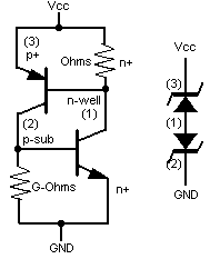
Figure 2: Bipolar model of a CMOS substrate
Clamp diodes are implemented into each chip to bypass overvoltage to either Vcc or GND. Due to the high voltage of electrostatically charged bodies, transient discharge currents are often between 2A and 8A, causing a substantial voltage drop across the resistance between the n-well and Vcc. This resistance can vary between a few hundred milli-ohms and a few ohms depending on the implementation of the device. As soon as this voltage drop forward biases the p+ to n-well junction (here modeled as a PNP transistor), base current drives into the NPN section, pulling even greater current through the n+ resistance, a run-away condition.
This shows the importance of having all input terminals terminated, so that charges can bleed off.
