1. Demonstration Kits
The DS2434 and DS2435 demonstration kits are, as the name suggests, demonstration kits. The programming option is fully functional for more than a few prototypes, however it is not only inefficient but will quickly reduce programming yields over time. This is because the socket wears out quickly since it is designed for non-repeating insertions. Although source code can be obtained from Dallas Semiconductor, it is advised to use these kits for demonstration or proof-of-concept prototypes only. The kits work under Windows 3.x or Windows95. Printed circuit board modifications are required for the use of a TO-92 style or 16-pin SSOP socket.
2. Serial Port Interface
2.1 Without a DS2480 1-Wire Bus MasterApplication Note 74, "Reading and Writing iButtonsTM via Serial Interfaces," explains in great detail the hardware and mechanical interface to 1-Wire devices. Dallas' Battery Identification ICs use a subset of the MicroLANTM standard, which means that they use the same communication protocol (transport layer) but differ with MicroLAN features such as addressability (network layer), overdrive, and programmability. Due to the nature of a limited battery pack supply voltage, non-volatile data is stored by using internal charge pumps rather than applying external 12V pulses.
Figure 1 displays a typical hardware interface that is used in our DS3701 Com-Port (?) adapter.
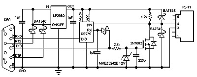
Figure 1: COM Port Adapter schematic
The 1-Wire protocol timing specifications require that the serial port is able to communicate at 115k baud. Because the 1-Wire GND terminal has to remain the voltage reference, the ordinary DS9097 COM Port Adapter cannot be used. During programming, supply 5V to the DS243x, which the DS3701 derives from the RS-232 line voltages. For the use with serial ports slower than 115kbps, a DS2480 has to interface between the serial port and the 1-Wire devices. This circuit is outlined in the following paragraph.
2.2 With a DS2480 1-Wire Bus Master
The DS2480 Serial 1-Wire Line Driver is an RS-232-to-1-Wire bus master. Its communication speed is programmable from 9,600 baud (default) to 115k baud. Because the DS2480 uses an internal timing generator, it releases the PC from being the timing source. The DS2480 interfaces directly to the serial port and receives the exact commands that are directed to the 1-Wire device. Then it converts the data byte into a 1-Wire bit stream, or buffers the incoming bit stream until the serial port is ready to receive the data. This simplifies the programmer development to raw data exchange without timing overhead and restrictions. As Dallas' DS0621-SDK Software Development Kit may be already at hand, fundamental "Touch" -I/O commands can be used to build the transport layer. This boils down the two functions Touch_Reset, and TouchByte, as the 1-Wire bus can only assume one of the following six states: RESET, PRESENCE, WRITE_0, WRITE_1, READ_0, AND READ_1. The idle state should always be logic high. However, the entire kit, with its overhead of iButton functions, is overkill for such a project. Figure 2 depicts a typical schematic for the interface.
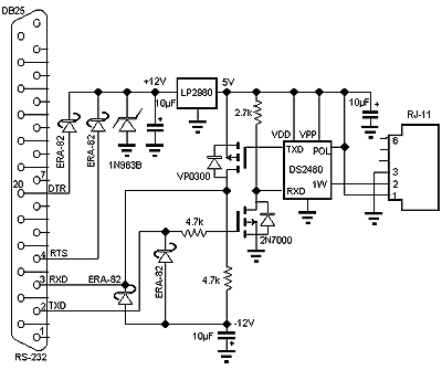
Figure 2: COM port adapter with DS2480 Bus Master
Programming more than one device at a time requires a stronger power supply than the supply through the serial port will provide. Although Pin 1 of the RJ-11 connector provides 5V through a low dropout linear voltage regulator, consider an external power supply for supporting multiple devices. This applies to gang-programmers, as the write process to EEPROM plus drive current for the (optional) LEDs will consume considerable power (Figure 4).
3. DS1481 Parallel Port Interface
NMI interrupts of the PC will not guarantee flawless communication to a 1-Wire device through a parallel port directly, and is discouraged to attempt. As the 1-Wire protocol requires the first 15us of each time slot to contain the data information, any disruption of this time segment will result in a communication error. Communicating through the PC parallel port, as it has been utilized for Dallas' DS1701K Thermal Demo Kits, requires timing corrections. These functions are performed by the DS1481 bus master. It translates code from the parallel port to the 1-Wire data line and buffers data coming from the 1-Wire device to the parallel port:
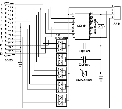
Figure 3: Parallel port adapter as used with the DS1820K
Programming through the parallel port may seem complex, but it still is a useful alternative when no serial port is available. Power can be supplied through the parallel port, which is often referred to as "parasite power." Schottky diodes feed current into a 22uF storage capacitor.
4. Standalone Microcontroller
The function of a DS2480 can be entirely emulated with a microcontroller. Source code patches for the following processors are available:
- Intel 8051 and derivatives
- Motorola 68HCxx
- Microchip PIC series
- Hitachi 6303
This source code enables a 1-Wire bit stream and covers all fundamental six states of the 1-Wire data line:
- 1. Reset
- Presence
- Write_0
- Write_1
- Read_0
- Read_1
All commands will use these six functions as sub-routines since the sequence of a 1-Wire protocol is given:
- RESET
- PRESENCE (detect)
- ROM command plus data - identifies a 1-Wire device
- function command plus data (receive or transmit)
While the two previous programmer solutions are using a "bus master" for correct timing, this approach must pay attention to the protocol standards. During bit transmissions, do not allow interrupts. In between two bit transmissions, the idle state of the 1-Wire is high and interrupts may be serviced. Unless a RESET is issued which resets the internal data pointer of the 1-Wire state machine, the protocol picks up where it left off.
5. Custom Part
A pre-programmed chip will solve the needs for developing and maintaining a 1-Wire programmer. Additionally, there will be no yield loss because programming occurs at the factory. Dallas Semiconductor requires a minimum order of 5,000 pieces for any custom Battery Management IC. A non-recurring engineering charge (NRE) charge may apply in addition to a small adder on top of the standard component cost.
6. Hardware Interface
While the next generation DS2436 and DS2437 utilize their unique 64- bit ID code to allow only one device at a time to talk to the 1-Wire master, the DS2434 and DS2435 need a DS2407 Addressable Switch to facilitate communication.

Figure 4: Hardware interface for programming DS2434
Switch PIO-B connects the GND connection of the DS2434, similar to the branching technique explained in Application Note 106. When the internal FET is turned on, the DS2434 can read from the DQ line and receive or transmit data. Switch PIO-A is used to send a visual alert when device programming failed. Thus it is easy to physically locate the faulty unit on the gang programmer board. Since all outputs are open drain, a 10k pull-up resistor pulls the gate of the external p-channel FET high (in-active), turning the LED off.
Because twenty or more LEDs can consume significant current, consider a PCB layout that uses a star-type current return path. Having the high current return separated from the low current GND reference of the DS2407 will promote safer communication due to increased logic low level margins.
7. Programming the Software
Using the addressable switches to program 20, 30, or even 50 Battery Identification ICs is simple because all PIO-B switches can be turned on at the same time. The verification process, however, requires that only one PIO-B switch is turned on at a time. This will prevent data collision when the battery identification IC is talking back to the 1-Wire bus master. First of all, before any devices can be programmed, each DS2407 has to be polled for their unique address code with the SEARCH_ROM command. Note that at this time all DS243x devices are disconnected from the bus. The LSB first protocol then executes three read time slots to retrieve one bit at a time with the following syntax:
- Read Bit_0 of all devices
- Read the inverse bit_0 of all devices
- Write either '1' or '0', depending on the outcome of steps one and two
| 1st read | 2nd read | result |
|---|---|---|
| 0 | 0 | devices with bit_x = 0 AND devices with bit_x =1 are connected to the bus |
| 0 | 1 | all devices connected to the bus have bit_x = 0 |
| 1 | 0 | all devices connected to the bus have bit_x = 1 |
| 1 | 1 | not valid - check for software/hardware errors |
Table 1: SEARCH_ROM results for each bit of the 64 bit ID
During the third time slot, the DS2407 is reading information: it turns itself off if this bit is not equal to its ID bit. It stays on-line if this ID bit equals the third time slot (write cycle). If devices with either bit state are present, you need to select one state and, after completion of this ID branch, repeat the procedure with the opposite bit logic state. This bit screening routine is performed for each one of the 64 bits. Once each DS2407 has been identified, either store this information in nonvolatile memory or make this procedure part of the power-up routine for the programmer. The MicroLAN protocol supports a data rate of 16.3kbps. This will enable the bus master to find up to 70 1-Wire devices per second.
You can broadcast programming data to all the DS243x devices at the same time provided all PIO-B switches are turned on. Then turn all switches off, and turn one at a time back on using the MATCH_ROM command. Verify programming of the DS243x and when unsuccessful, either retry programming or turn on the LED through PIO-A of the same DS2407 for visual indication.
8. Programming With a DS2480 Bus Master
The DS2480 supports 1-Wire communication through the serial port at any baud rate. Its design incorporates a "SEARCH Accelerator." This feature increases the speed to find all participating 1-Wire devices on the bus from about 40 to about 180 devices per second. Since all participating devices are of the same family, a significant amount of this address remains constant and helps finding the remaining addresses more quickly.
On command, the DS2480 receives and retrieves 16 nibbles of actual ROM address and sixteen nibbles of a verifier called "discrepancy bit" or here, D-bit. These 16 bytes make up two sets of eight bytes, which then have the following structure:
| 7 | 6 | 5 | 4 | 3 | 2 | 1 | 0 |
|---|---|---|---|---|---|---|---|
| R3 | D3 | R2 | D2 | R1 | D1 | R0 | D0 |
Table 2: Search Accelerator byte (LSB) - one out of sixteen
After the data mode of the DS2480 has been selected with [E1h], send 16 bytes to determine the logical decision path in the event of a logical conflict. This occurs when either logic value of the same address bit is present on the bus. Because the D-bits are not encountered during a write process to the DS2480, these bits are DON'T CARE terms.
Start to perform a Search ROM sequence with all bits Rn being 0s. The returned bytes will flag the exact bits of the 64 bit address, which contain both, logic 1 and logic 0 states.
| Bit no. | 7 | 6 | 5 | 4 | 3 | 2 | 1 | 0 |
|---|---|---|---|---|---|---|---|---|
| type | R | D | R | D | R | D | R | D |
| shift-R div.by | 7 128 |
6 64 |
5 32 |
4 16 |
3 8 |
2 4 |
1 2 |
0 1 |
| ROM D-BIT | R3 | R2 | R1 | R0 | ||||
| D3 | D2 | D1 | D0 |
Table 3: Unwrap nibbles from LastReceived of the DS2480
The first byte will contains the lower nibble, the second byte will contain the higher nibble of the ROM code.
Repeat this process until you find the highest number D-bit. Since each process starts with determining the address in the event of a discrepancy, the selection will branch out from the higher address to the lower address. This recursive iteration is illustrated in Figure 5.

Figure 5: Using the Search_ROM function with a DS2480 bus master
The flowchart in Figure 5 illustrates how to perform the Search_ROM function using the DS2480's Search ROM Accelerator. The notes below follow along with the flowchart to the left. If in Command Mode, the DS2480 will send a RESET to the 1-Wire port, and return either [C5 h] or [E5 h] when at least one 1-Wire device has been recognized.
When turning the accelerator ON, discard the echo of [F0 h] which the DS2480 produces when searching for 1-Wire devices.
This routine checks for the highest order discrepancy bit that is flagged (logic high). Note that all 1-Wire communication is LSB first.
TCurrDiscNum is the current discrepancy number. Perform the discrepancy test with a logic AND function with 55 h. This screens out all ROM code bits and retrieves all discrepancy bits from the code received from the DS2480.
This inner loop is repeated for all 16 bytes, which contain the 8-byte ROM code and the discrepancy bits for each bit location. Build a discrepancy history by selecting first all "zero" addressed devices then continue with all devices containing a "one" in that flagged location.
(*) If there is no discrepancy at all, but a 1-Wire device has signaled presence to the DS2480, obviously there only one device on the bus.
"Unwrap" the nibbles of each ROM-Byte into ROM code and discrepancy bits.
Note that each byte contains a nibble for the ROM code and a nibble for the discrepancy bits. Consequently, the first byte [j] contains the lower nibble and is shifted right. The second byte [j+1] contains the higher nibble and is shifted left. Eventually all eight bytes are OR-ed to yield the ROM code for the particular device. These functions are easily implemented in a C-based language, since C supports bit manipulation functions such as SHIFT RIGHT (>>), SHIFT LEFT (<<), logic AND (&) and logic OR (|).