
by N2CEI, Steve Kostro
PREFACE
For anyone that considers themselves a VHF/UHF/Microwave
enthusiast, sooner or later you will repair or construct a low
noise preamplifier. It may be a handbook design, a kit, or you
best friends favorite LNA that needs to be repaired. It doesn't
matter ! You will need to have some basic technical skills in
order to achieve some kind of favorable results.
Maybe you are just a casual VHF'er and you
think that you receiver performance could improve with the use
of a LNA but don't want to buy a new one to find out. I am sure
there are some good LNA's in the junk boxes of many hams that
have been given up on. There have been many broken LNA's sold
at local Ham flea markets by individuals that have thought, "I
couldn't fix that other one, might as well re-coup some of my
losses now!" Well maybe that's not a bad thing. With the
cost of the best GaAs FET's ever produced being the lowest price
they have ever been, it makes a broken preamplifier at a flea
market a bargain!
What will be discussed in this paper are some
designs thoughts, troubleshooting techniques and some basic rules
for biasing, tuning and operating. This will require a basic circuit
knowledge of LNA's and some circuit descriptions to determine
what type of preamplifier you may have to repair or want to build.
LNA'S
TYPES
I like to break down all LNA's into categories.
I categorize the Gate circuit, (Input) , the Drain circuit (output)
and the Source circuit. Having a basic understanding of the different
circuit designs will help in deciding what is best for your situation
or to help in repairing a preamplifier that doesn't operate correctly.
Having an understanding of the different circuits may also help
make a determination of why a perfectly good preamplifier tested
with a noise figure meter does not function in your station.
INPUT CIRCUITS
The input circuits are straight forward in
their descriptions. All LNA's have some sort of adjustment on
the input circuit to optimize the gain and noise figure. Some
are very minimal such as a series inductor. These types normally
have the lowest noise figure but have a very broad pass band.
They are the simplest and most popular preamplifier for microwave
use. The RF portion of the input circuit looks like this.
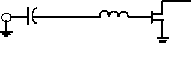
The bias circuits are not shown because in a correctly designed input circuit, they are de-coupled from the RF circuitry and simply supply a negative bias voltage or provide a DC path to ground. They should not provide any matching. Grounds are may either be DC, RF, or both.
A second type of input circuit is normally
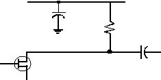
found in VHF and UHF LNA's. It can be called a Series C Shunt
LC circuit. This is a simple resonate circuit of the frequency
of choice that also provides a basic noise match into the FET.
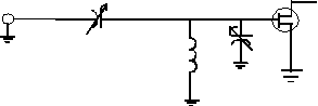
The shunt C that is shown in this circuit is
optional. Having it will provide a little more selectivity and
is recommended although it will degrade the Noise figure at higher
frequencies. More components, more loss!
SOURCE CIRCUITS
One type and the most popular is self biasing
source circuit. Self biasing is used on lower frequency LNA's.
(1.3 GHz. and below) On LNA's that use series inductor input
circuits, some inductance is required on the sources. This inductance
helps provide a better input match on the preamplifier. The by-pass
capacitors provide the RF ground terminating the source inductors.
Another type of biasing is negative gate biasing.
It may be used on any frequency preamplifier but does not
provide any benefit below 70 CM. When using negative biasing,
the source leads are always on DC ground. The higher the frequency,
the more critical the grounding as any length of the source lead
from the package of the FET to the ground termination, will look
electrically like a inductor. This is why LNA's are modeled with
inductors in the source to ground path. It is also shown on most
schematics even though it is a DC and RF ground.
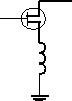
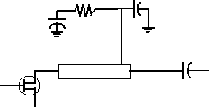
DRAIN CIRCUITS
There are many types of drain or output circuits
that are used. The goal in the past has been to design a circuit
that will match the FET to 50 ohms without losing much of the
gain it has developed. This is why older design low frequency
LNA's will have baluns in the output circuit. Higher frequency
LNA will have tuned resonate circuits, and microwave LNA will
have ¼ wave matching stubs. All of these circuits were good
in their day. Modern day Drain circuits will have resistive
loading drain circuits the supply the bias.
Resistive
loading provides a stable match (S22) across a wide frequency
range. Baluns and resonate circuits have a imposed frequency limit
and both have a mismatch out of band. This in turn will degrade
the IP3 performance and may cause problems if a filter is placed
in line after the LNA. Most energy that is reflected back from
a filter will be absorbed in the resistor load
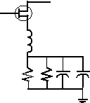
Modern day Microwave LNA's use resistive
loading in a different fashion. The loading is used to swamp
all but the design frequency gain. This is done with a ¼
wave bias line (a choke) with the DC supplied through a 50 ohm
resistor that is by passed with a large value capacitor.
This design is now what is used on most PHEMPT
LNA's. The circuit works great if the Gate and Source circuits
are correct. But! With even the best designs, problems will occur
if some fundamental steps are not taken.
PREAMPLIFIER OSCILATIONS
The general perception of oscillations in LNA's, is that they are caused by many different factors. The true cause is that the output to input isolation becomes equal to or less than the gain of the FET. A feed back path will develop and a instant 100mW signal source is born! The causes of these feed-back paths may be different for different designs. The good news is that with today's FET's having input to output isolations as great as 40 dB, feedback paths can be prevented!
VHF and UHF
LNA's (50 - 450 MHz.)
In VHF and UHF LNA design, using lump circuitry
is a mainstay. It is simple and cost effective. One or two tuning
elements for easy adjustments and the LNA falls into spec. Simple
construction techniques and repeatability are easy for production
and produce high yields. So how about repairing one of these
or building one from scratch!
First verify the design. For VHF/UHF, source
biasing is the easiest and the best. A input circuit with a series
C, shunt LC, is recommended with the added RF pollution that exists
today. The output circuit should always be resistive loaded.
If the design you want to use or repair has a balun, consider
replacing it. An added benefit by replacing the balun is that
baluns radiate. Eliminating this radiation will improve isolation.
This is helpful if the FET that you are now using has more gain
than the previous design.
A considerations in repairing a LNA is that if you change the FET, change the source by-pass capacitors if you have any doubts of their condition. A LNA that works fine for a long time and then develops and oscillation is most likely cause by the source by-pass caps. Mount the source by-pass caps as close to the body of the FET as possible. If you have a series input inductor circuit, the bypass caps were spaced at a certain distance from the FET body. Do not repeat this! Mount the caps close to the FET and change the input circuit! Below is and example of a finished product.
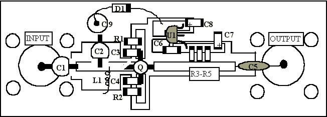
The input circuit is C1, C2, and L1. It a series C, shunt LC. Their values depend on frequency of operation. The drain circuit is resistor loaded. R3-R5 are used in this example. The FET is biased for high current, The standard dissipation for a 1206 size chip resistor is 1/6 of a watt. 3 of them will dissipate a ½ watt. A single 1/2 W carbon composition resistor may be used. With the value of the drain resistor being around 100 ohms, and C6 being a RF short at the design frequency, it provides extra isolation and stability. It also has attenuation and sometimes not enough. Additional attenuation may be needed on lower frequency LNA's. A series resistor may be inserted before C5. The RF is coupled out with C5. The source bypass capacitors are C3 and C4 and should be around 1000 pF for 50- 450 MHz. The source resistors, R1 & R2 can be any kind of resistors if the source capacitors are doing their job. But the source caps, can't work if the grounding is not adequate on the circuit board. The supplied regulated voltage in this case is 9 volts. This FET is biased for 60 ma. By adjusting R1 and R2.
The voltage is then dropped across the 100
ohm resistor to produce 3 volts on the drain of the FET
Possible problems in this design besides
bad by-pass capacitors, is the construction of the input circuitry.
Keep all connector pins as short as possible. Be sure to keep
the input inductor as close to the circuit board as possible.
Also shorten the leads of the variable capacitor as much as you
can. Small ceramic trimmer are fine for frequencies under 450
MHz. A sign of the input circuit radiating is when the gain and
noise figure change when the cover is installed. Bad by-pass capacitors
can be detected if the LNA changes gain or Noise figure if a metal
object such as a tweezer or small screw driver is placed on the
source leads. Try it!
If a better noise figure is desired, lower
loss piston trimmers capacitors and a less resistive inductor
such as a larger diameter wire or brass strip may be used. Some
exotic designs using copper pipe or waveguide for the input inductor
lower the noise figure even more if you do not have a space limitation.
For practical reasons, it would not serve any purpose but to win
a noise figure contest and to be used on 70cm EME.
LOW FREQUENCY MICROWAVE LNA's (800- 1700
MHz.)
LNA's in this frequency region are a design
hybrid. Microstrip and lump components work together. Because
of circuit radiation, the microstrip techniques are used to transfer
signals from one point to the other. Using axial leaded components
to connect the circuit board to the RF connectors are not recommended.
For manufacturing, this simplifies the assembly process. Circuit
boards can be assembled, tested, then installed in a enclosure.
Circuit designs can vary. If noise figure
is not a factor in the design, series C, shunt LC circuits can
be used but if variable capacitors are used, the design becomes
expensive compared to fixed value chip capacitors. There will
be designs like this in the future for the 33 and 23 CM amateur
bands. The designs will be a compromise of selectivity and Noise
figure but because of spectrum pollution, it will be the only
way we will be able to operate these bands in the future.
For now the Series L input circuit is the
most popular. It will produce the best noise figure in a LNA because
it has the least amount of loss on the input circuit. Using this
type of circuit requires that you adjust the length of the source
leads of the FET to set the input VSWR of the LNA. Fractions
of a nanohenry are required! Then of coarse, the best microwave
type of by-pass capacitors are required to terminate the source
leads RF wise. Added inductance from a poor quality chip capacitor
at 1 GHz. can decrease the output to input isolation of the FET.
No Good!
The drain circuit should be resistor loaded
for ease of assembly and stability. Using axial leaded resistors
are OK if they are carbon composition. Metal film or Carbon film
have metal end caps where the leads attach to the body and they
will radiate RF energy. Chip resistors work best! See the following
example of a low frequency microwave LNA component layout.
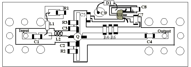
Some
important things to note about this design is the input and output
connectors make a direct connection to the circuit board. For
800 MHz and up this becomes necessary. The only frequency sensitive
element in this whole circuit is L2. This design can be made to
operate from 150 MHz through 3 GHz by changing the size of
L2 but is not recommended. C1 can be any low loss chip capacitor
but designers prefer to use the lowest value as possible to perform
some low frequency roll-off. The lower value capacitors also have
the least amount of radiation. L1 is a RF choke that is the DC
return of the gate circuit. This choke is not critical to the
RF design but it should be a small physical size and to be made
of some composition that will keep the RF radiation to a minimum.
R1 is a termination that absorbs all undesired energy under the
designed operation frequency. At least that's the theory!
C2 and C3 are the source by-pass capacitors.
They are shown in a position for 1.3 GHz. They should be 470
pF. Move them out for lower frequency, in for higher frequency.
Source resistors can be placed anywhere on the line. The Drain
resistors are shown as three 300 ohm chips. One 100 ohm ½
watt can be used if it is a carbon composition type. C5 should
be a good quality chip capacitor to cover a broad range of by-pass
frequencies. C4 is the output coupling capacitor. It doesn't
need to be a microwave type chip. A little loss in the component
won't hurt if it doesn't radiate much.
Potential problems with the design are poor
grounding on the source capacitors and correct positioning . The
positioning of the L2 inductor needs to be elevated off the circuit
board but not to far as to radiate when it is place inside of
an enclosure. Biasing is the same as with any FET. Depending
on the desired results it can be done the same as with the VHF
example. Lower noise figure can be achieved with lower current
drain but higher IP3's are possible with little degradation in
noise figure by biasing the FET's for power. Use the best quality
components as possible and keep all leads as short on the L1 choke
and drain resistor if you chose to use a carbon composition.
PHEMT LOW FREQUENCY MICROWAVE DESIGNS
With PHEMT designs, a negative bias gate supply is required to obtain lower noise figures than with standard GaAs FET's. But Caution! Designs of this nature do not work well under 500 MHz. Stability is still questionable at 1 GHz. To match the FET to 50 ohms, a large low loss air inductor is required. Its a potential isolation problem! A series L is the only way for low noise. Any added circuitry would achieve the same results as a standard FET. Designs 1.3 GHz. and up work fine. Examine the circuit below.
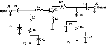
L1 and L2 are air wound inductors and L1 is
the frequency sensitive device. C1 needs to be low value and low
loss good quality chip cap. The assembly of J1, C1, L2, and the
gate of Q1 should be all assembled above the circuit board and
connections should be as short as possible. If not, the noise
figure will degrade. L1 needs to be twice as large in inductance
as L2 for starters. C2 should be a RF bypass capacitor at the
design frequency. R1 and C3 are low frequency loading and bypass.
R1 also provides a higher impedance to protect the gate supply
from RF.
Q1 source leads are on ground. You cant make
the source leads short enough! There will always be some inductance
and that is the reason for it being on the schematic.
PHEMT's have a lot of low frequency gain.
Most designs include a loading resistor (R2) in the RF portion
of the drain circuit. It provides added isolation and some additional
voltage drop. R3 and R4 can be what ever value is needed to obtain
the required voltage drop to the drain circuit. In this case R3
is a 50 ohm with a design frequency RF by-pass capacitor( C6)
for additional loading. R4 then becomes the adjustable value
to set the voltage. C5 is a low frequency by-pass. The signal
is coupled out of C6. It should be any type that doesn't radiate
at the design frequency.
Potential problems are that it is very difficult
to adjust and test with out a noise figure meter. Repeatability
at 1 GHz and below is not good FET to FET. Air wound inductors
are subject to interpretation. Selection of a drain loading resistor
controls the amount of gain and isolation. Other considerations
are lead length of resistors, inductors and the FET's source
leads. A design problem is that because of the high gain and
frequency of operation common to PHEMT's, a low frequency design
may be hampered by a high frequency oscillation. This will degrade
the noise figure by a few tenths of a dB and make one think something
else is wrong. Sometimes changing a cap a pF or two or stretching
an inductor will make it go away! These FET's were not designed
to operate in this frequency range. We make them comply! (sometimes!)
MICROWAVE LNA's 2 GHz. AND HIGHER
A few years ago when standard FET's were only good to 1.0 dB noise figures, a cheap circuit board and a few 0603 size chips caps got you on the air. With PHEMT's that produce better than .5dB noise figures a 10 GHz., the factors that limit hot designs are construction techniques, component quality, and PC board manufacturing. We are in the age where FET's are not holding us back! New terms such as Single layer and multi-layer capacitors, low inductance vias and circuit board materials that have replaced Teflon glass , will be utilized to maximize the potential of all of these new FET's. For now, because of economic reasons and lack of development time,
we can only use the thinnest PC board materials
and the best quality components as possible in designs up to 10
and 24 GHz. Do you have a wire bonder?
The designs that are available today are all
microstrip designs. They have printed chokes and matching circuits.
All circuits have resistive loading for low frequency by-passing.
Multi stage designs are common because of gain requirements.
The best noise figure and the easiest LNA to design or build
are single stage units. Its is recommended to put in extra tuning
stubs before cutting or etching a board. Also remember, there
is no such thing as too many vias! See example below of what is
the now the " State of the Art".
Simplicity in design is best. C1 is the coupling
capacitor. It should be a 50 mil porcelain or other microwave
low loss type and a RF short at the design frequency. After the
C1 cap, impedance matching takes place and the RF is routed
directly into the PHEMT. Notice the extra tuning stubs. The gate
bias is de-coupled from the matching network with a high impedance
printed choke and it is connected to a ¼ wave stub at the
design frequency. R1 is a 50 ohm chip that acts as a termination
for low frequencies that is by-passed to ground with C3. The printed
choke to C6 is a bit redundant, by doesn't hurt the design. The
schematic doesn't show the extra choke.
R3 is a load resistor. It provides attenuation
and isolation along with some drain voltage drop. R3 , (15 ohms
or so) is what the FET sees across it's whole spectrum. The signal
continues into the output matching network and is coupled out
through C2. This capacitor doesn't need to be the best capacitor
in the house, but you don't want it to radiate. Then just like
on the gate bias circuit, the drain bias is supplied through a
printed choke but is by-passed with a chip capacitor this time.
This needs to be a good Microwave cap at the design frequency.
R2 is a low frequency 50 ohm load resistor and is by-passed with
C5. C7 provides lower frequency by-passing yet. R4 is the resistor
used to set the Drain voltage.
As the circuit board layout shows, the RF
connectors are mounted directly to the PC board. This provides
the best results but the board needs to have some other support
to prevent flexing. The flexing will break the chip components
and the ground vias. This is the most common problem with microwave
design LNA's. Other problems can be the selection of components
and proper biasing.
SHF LNA'S
With FET's becoming available with higher
operating frequencies, new designs are showing up at 24 and 47
GHz. These designs seem to be exotic but in reality are quite
simple. Eliminating losses on input circuits by using coupled
lines or direct bonding to a chip will be the way to optimize
noise figures and gains at these frequencies. A 1 dB noise figure
on 24 GHz is not that far away for amateur use . MMIC's that are
based on PHEMT's for 24 GHz are available now with noise figures
around 2.0 dB. And they are economical to boot! These same MMIC's
will produce 1.0 dB noise figures and 20 dB gain at 10 GHz. And
the industry will make it better !
LNA BIASING
Danger High Voltage and Voltage Kills are
the theme for any type of GaAs FET. Maximum drain voltage for
Standard FET's are about 5 Vds.( Voltage drain to source) With
source biasing the drain can withstand about 6 volts directly
without flashing over. If you use a grounded source, the maximum
voltage is now 5 Volts.
For the lower frequency LNA's, the standard GaAs FET's will operate best noise figure around 20 -25 ma of drain current, This also requires a minimum of 2 volts on the drain. Adjust the source resistors to obtain the current drain spec. If the Drain voltage drops much below 2 volts, then there is too much resistance in the bias line. If the voltage is to high, add resistance.
A new trend in LNA design is to bias the FET's
much higher in current. When doing this, the drain resistor need
to be re-adjusted to a lower value and the regulated drain supply
voltage will need to be higher. Most FET's that are biased to
60 ma. Will require a 9 volt regulated supply. This voltage is
dropped through a 100 ohm resistor. A little high in current and
a little higher in Drain voltage will produce a LNA with a much
higher resistance to over load and its susceptibility to intermod
with a slight to none degradation in noise figure.
With PHEMT's the voltage maximum is lower. Drain voltage is +3 volts and the gate voltage is -3 volts. The differential needs to be less than 6 volts. So with a grounded source, any bias supply that is used should be pre-set to -1 volt or less on the negative supply. This ensures that even if the drain supply comes up at 5 volts, the FET will draw some current and drop the voltage across the drain loading resistors enough not to flash the FET. Setting the negative supply to 0 volts is better than -5 volts! Do the math!
If the design is sound and the construction
and components used are top notch, then you will have a high
quality LNA. The low frequency models will require adjustment
to the RF circuits. The Microwave LNA will require bias adjustment
and maybe a "tweak" or two. If you have a chance to
test your LNA on a noise figure set-up you should. It will give
you an idea what is required to achieve certain results.
IT'S WORKING !
So now! How do you keep this LNA working perfectly?
First! Did you clean all of the flux off the circuit board?
This should be done before testing but sometime bias changes or
circuit modifications while testing happen and the circuit board
should be cleaned before final test. If the LNA is to be used
in a harsh environment, any moisture can activate the flux residue
left on a circuit board. This will eat its way through circuitry
and by-pass capacitors.
Be sure of your transfer relay's isolation
and if you sequence the transfer, do a dry run with a dummy load
in place of both the RF and the DC. Verify that the voltage doesn't
drop with the current drain. If you operate multiple bands, verify
the power your LNA will receive if a different frequency transmitter
is used. ATV, Satellite and Contest operators are amazed sometimes
when the find out what was blowing out their LNA.
There are many other possibilities for LNA
damage. Think it through before wiring it in line and verify power
supplies, coax cables, and relays before using. It could save
you a lot of time.
CONCLUSION
I hope this will help some and provide encouragement
for others to tinker, design or repair LNA's in the own shacks.
It can be fun and rewarding and you never know! If you have that
hot design-------------------
Good Luck and enjoy the hobby as much as I do.