
General overview of the interior.
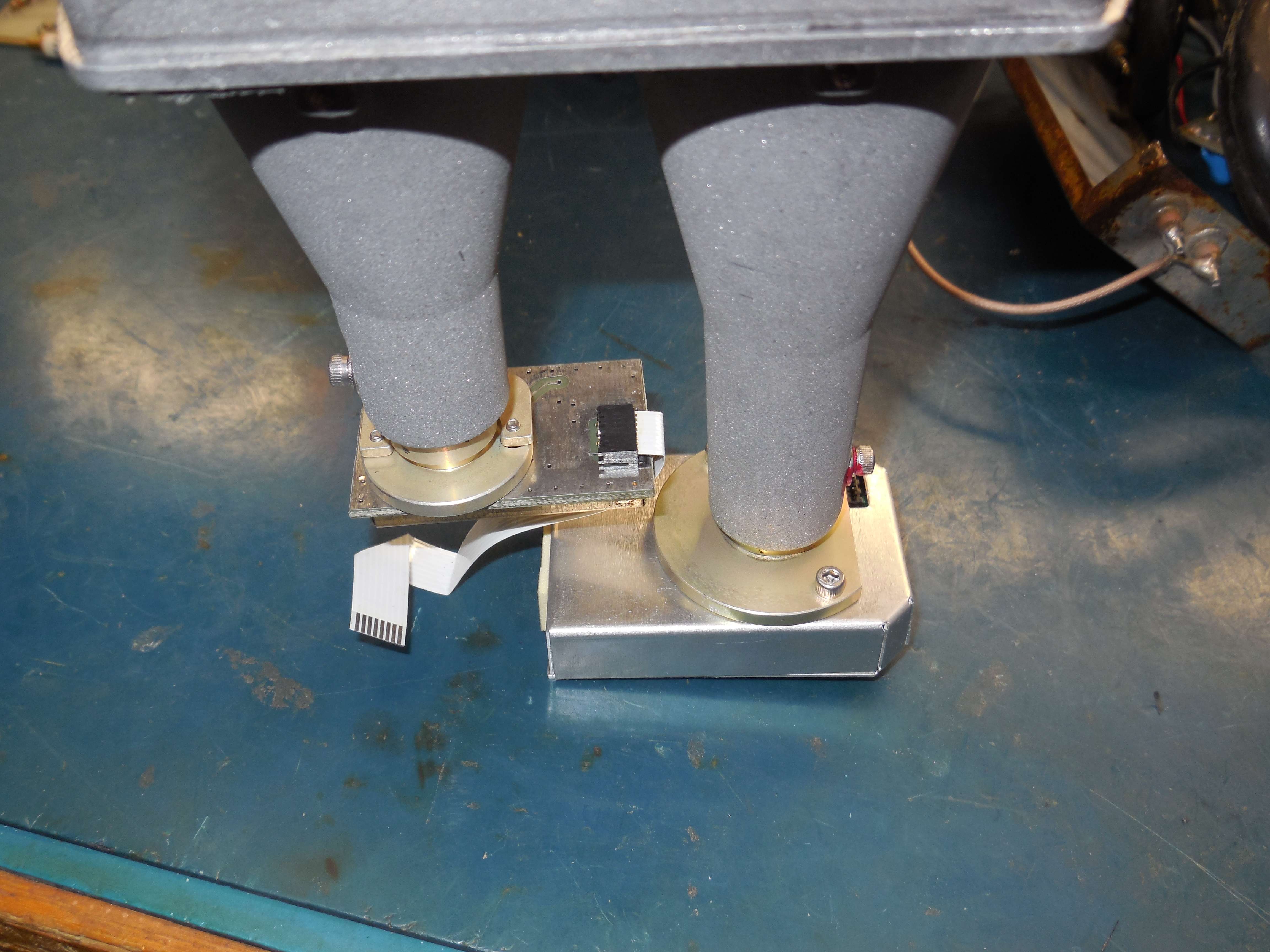
The "long" tube is the receive section containing a PIN photodiode.
The "short" tube is the laser diode and pulsing circuit.
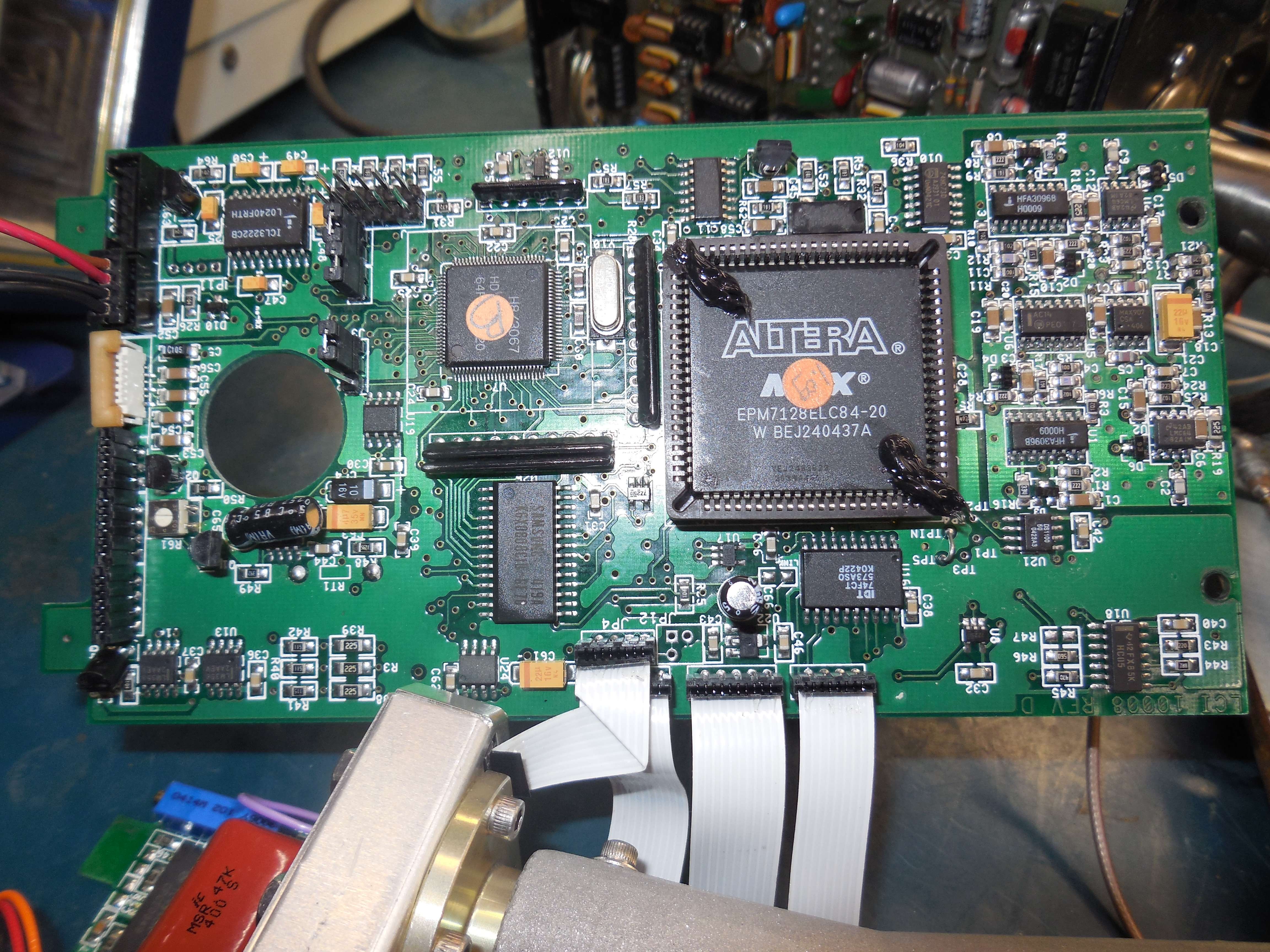
Main processing board.
There is a program/run jumper (J3).
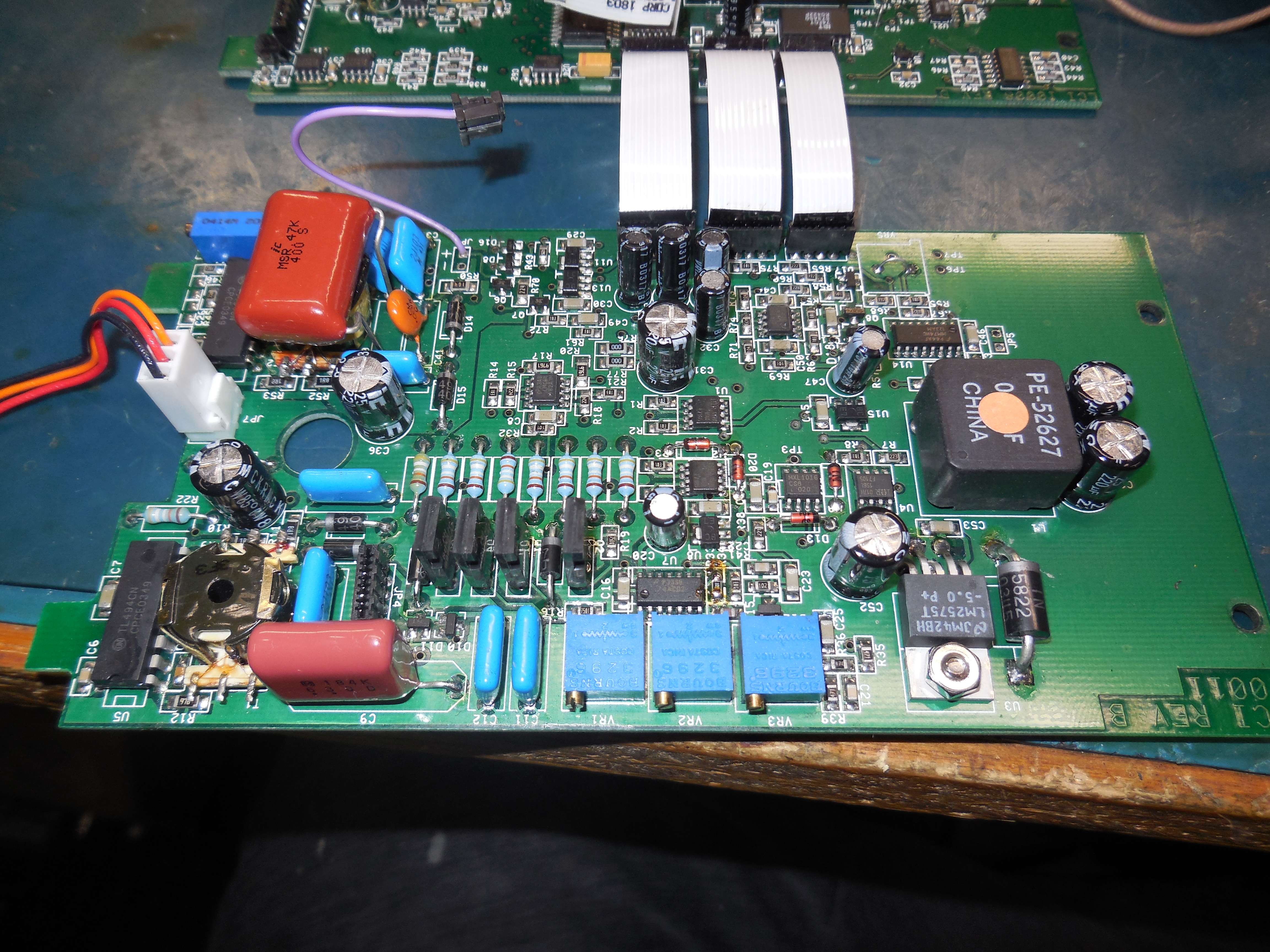
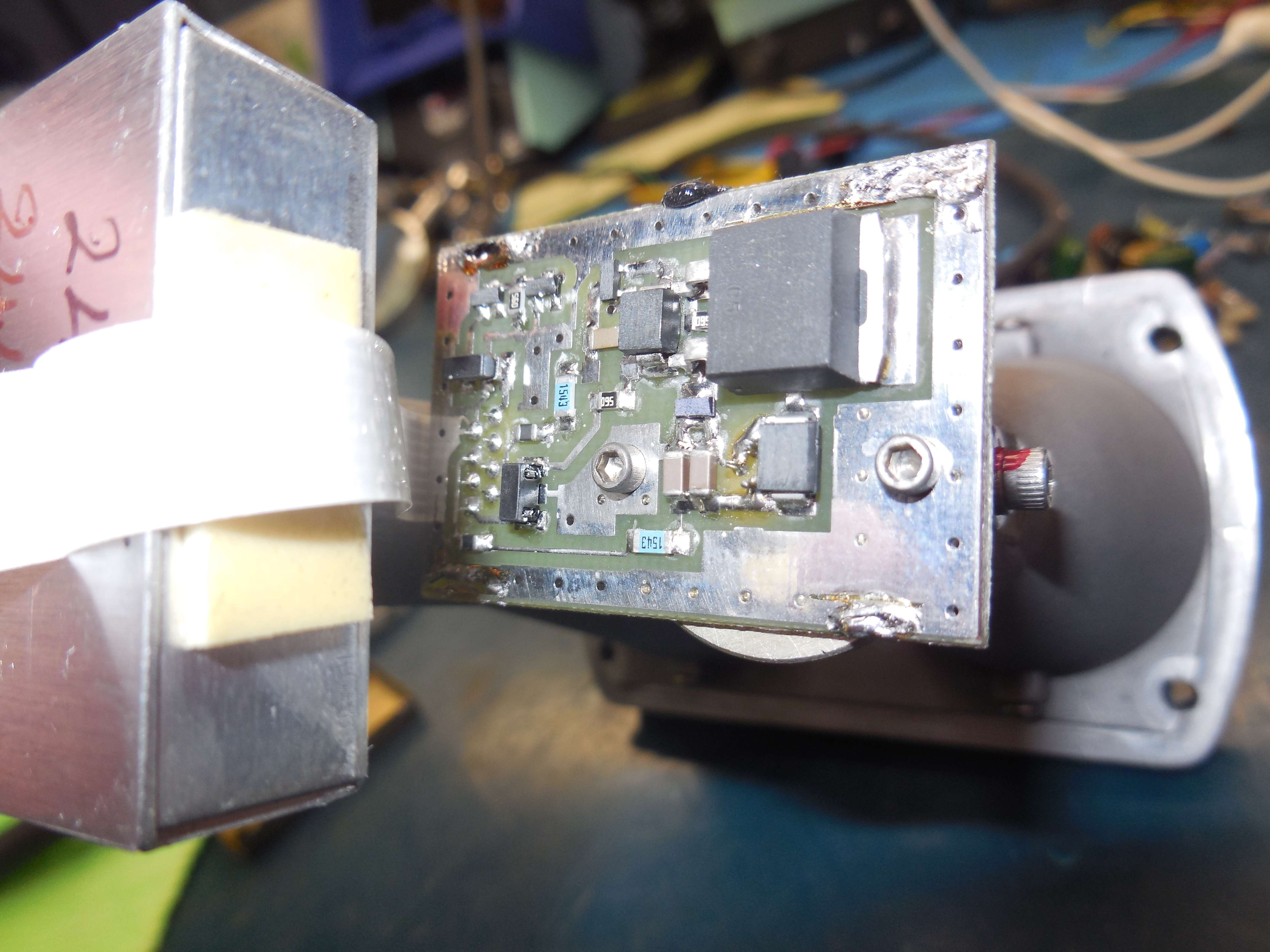
Power supply board.
High voltage on the upper-left.
Low voltage along the bottom.
The laser diode module connection (JP4) is near the large reddish capacitor along the bottom.
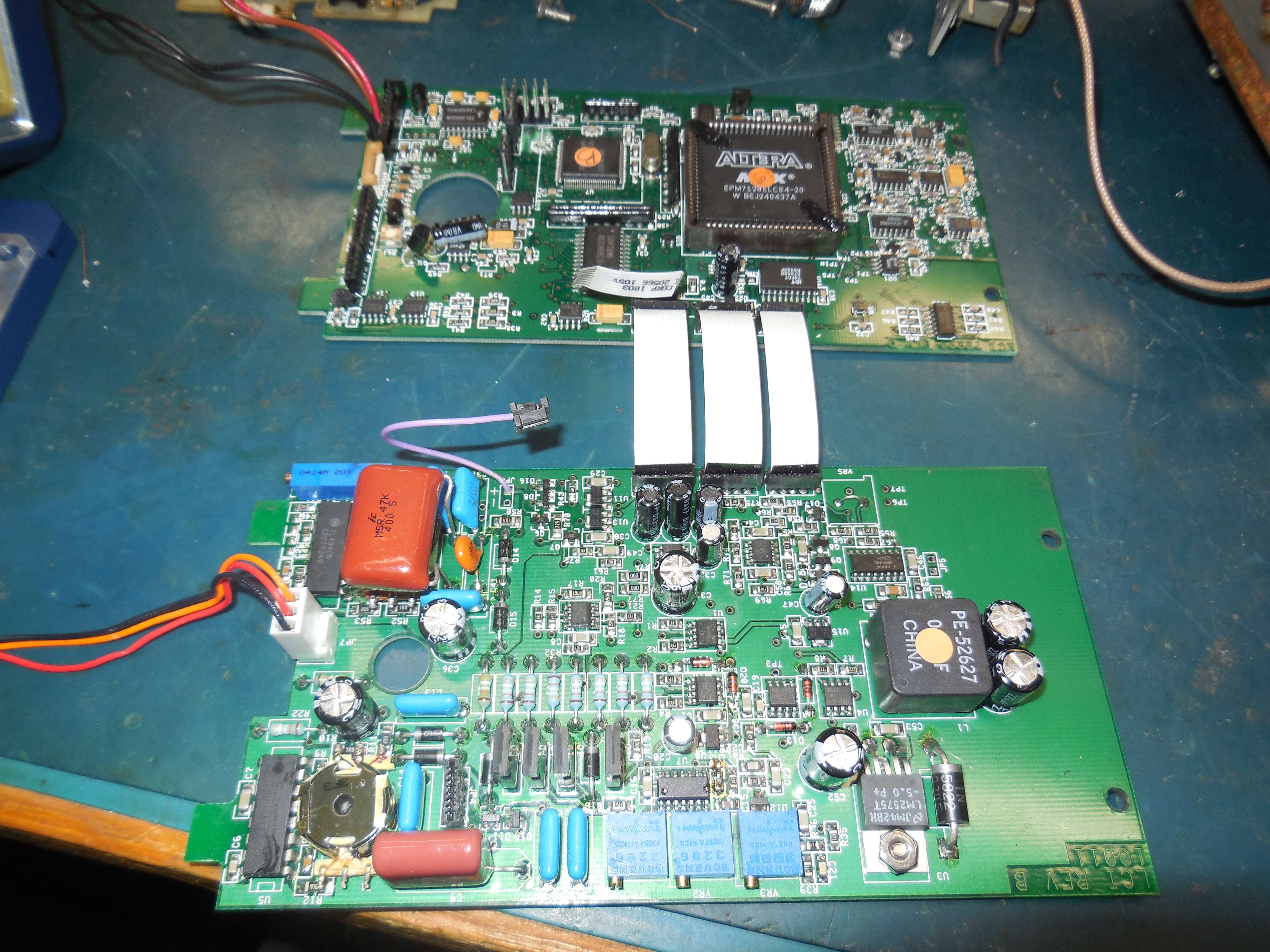
Overview of both PC boards.
The main board is on top and the power supply board is on the bottom.

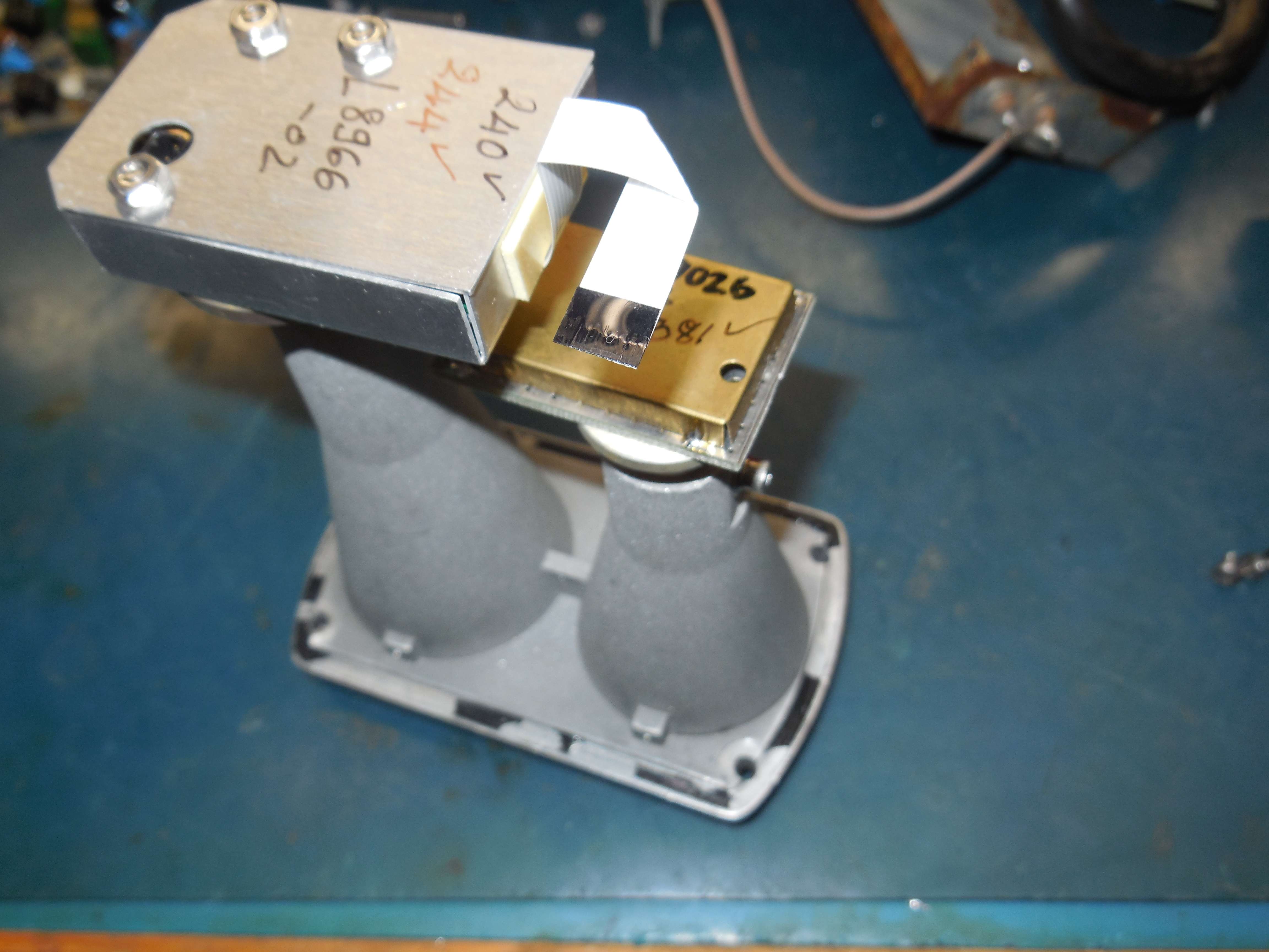
The receive PIN photodiode module is on the left.
The purple wire is the +450 VDC bias for the avalache PIN photodiode. It's matching high-voltage DC-to-DC switching power supply is the section on the lower-left.
The PIN photodiode module has the following writing:
240✔ 244✔ L8966-02 |
The laser diode module is on the right.
The laser diode module has the following writing:
LX9026 HUX 381✔ |
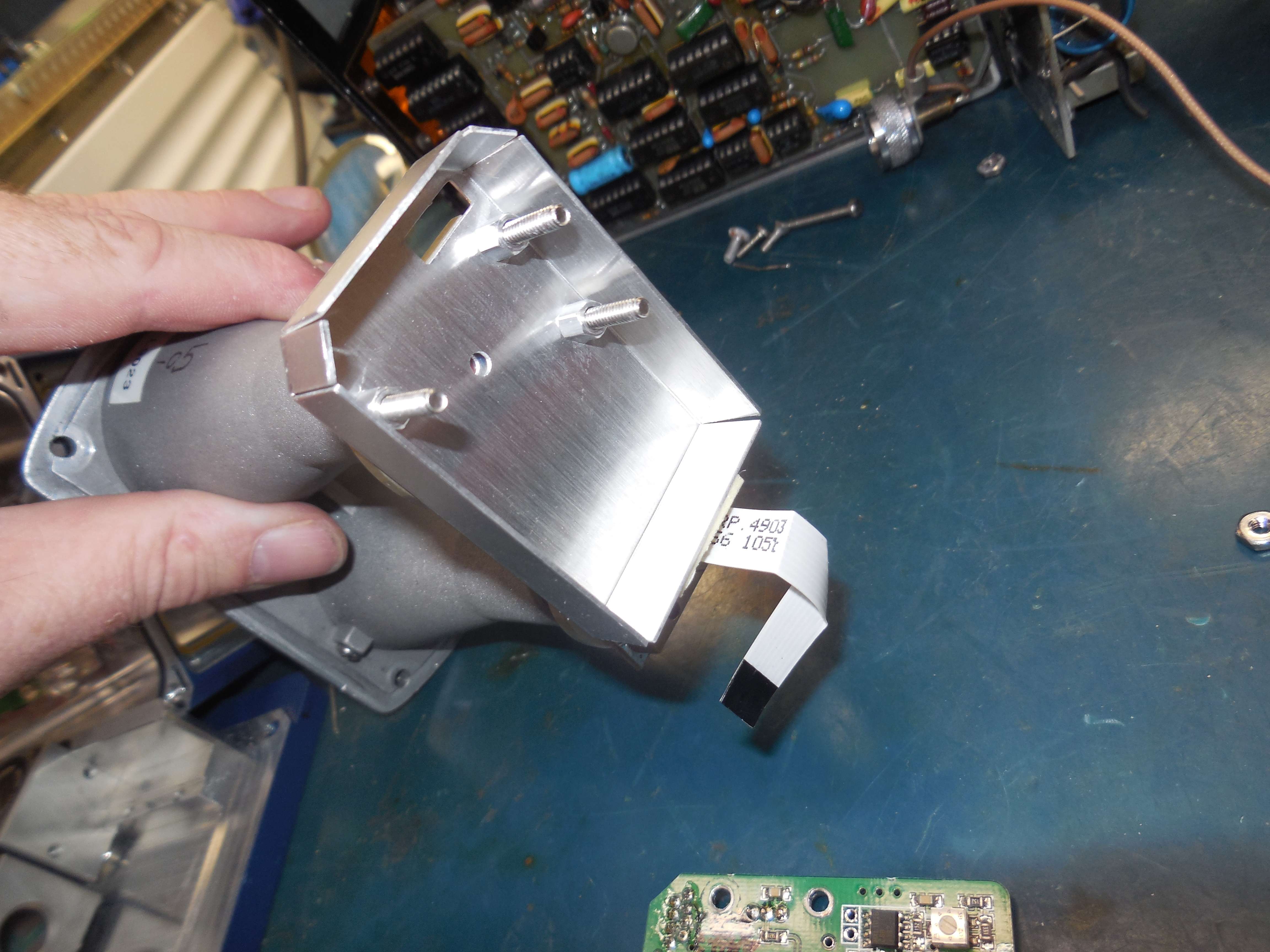
Looking at the rear of the optic tubes.
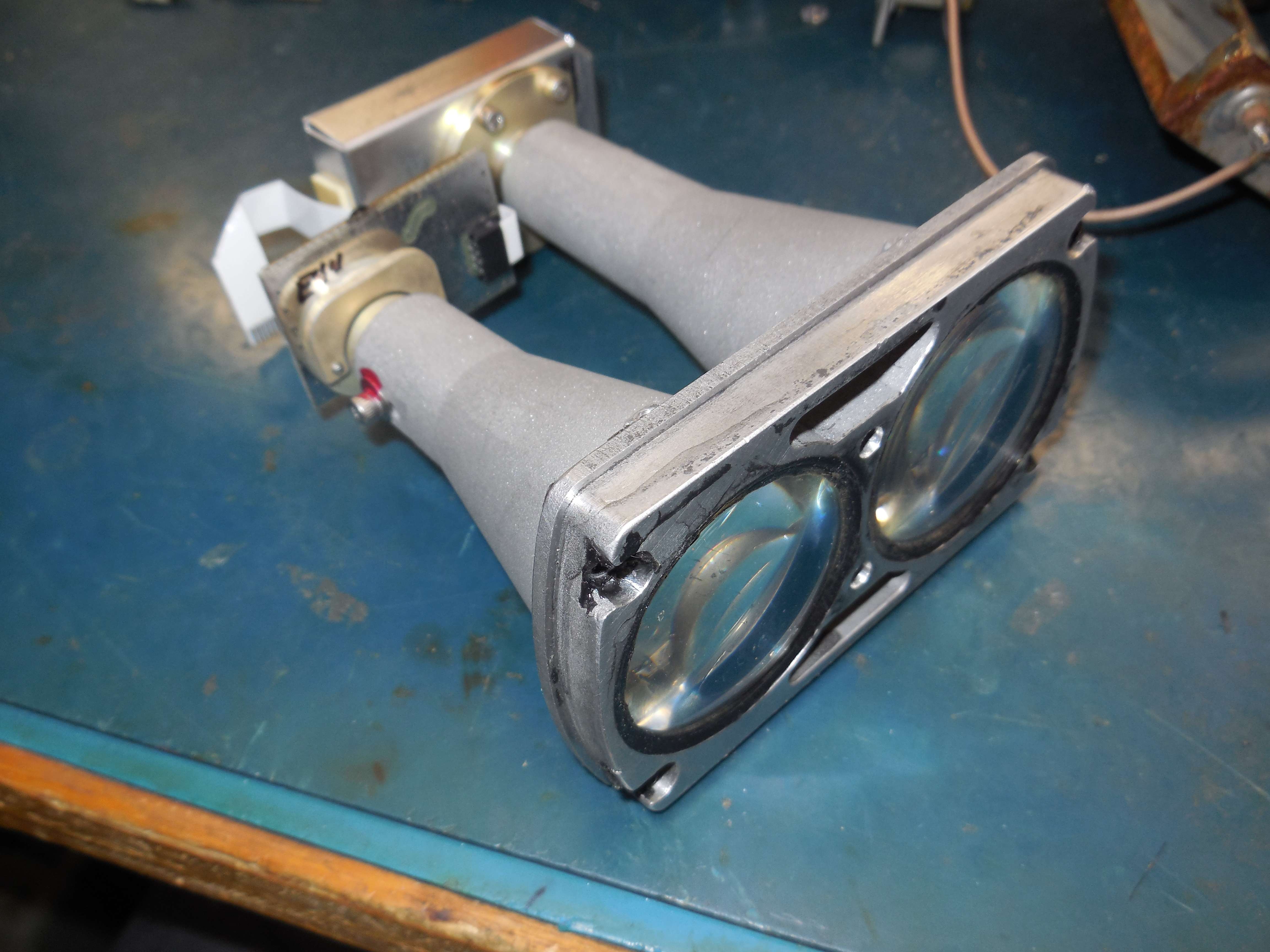
Alternate view showing the lenses.
DO NOT loosen the Allen screws with red markings or the focusing will get messed up.
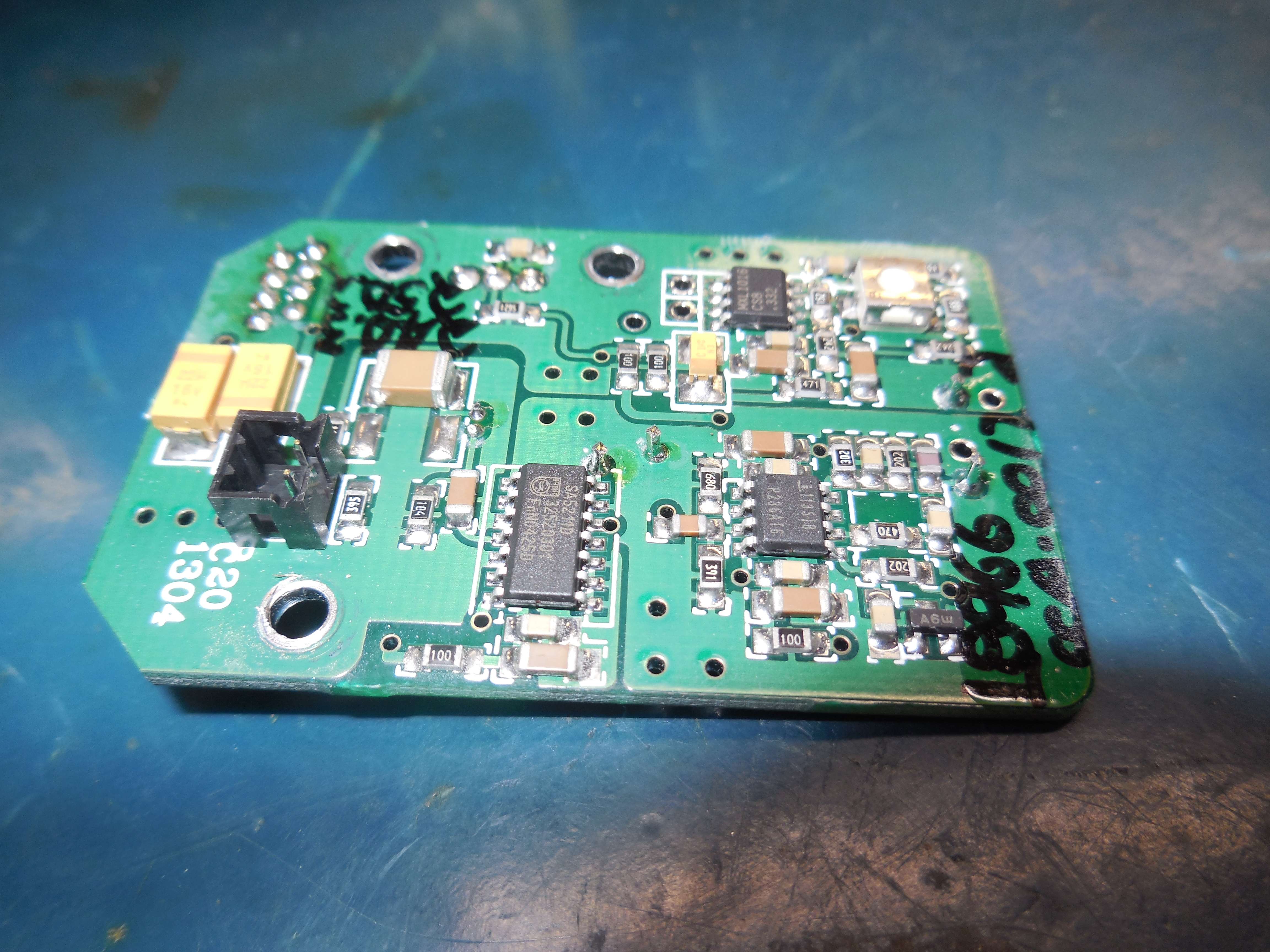
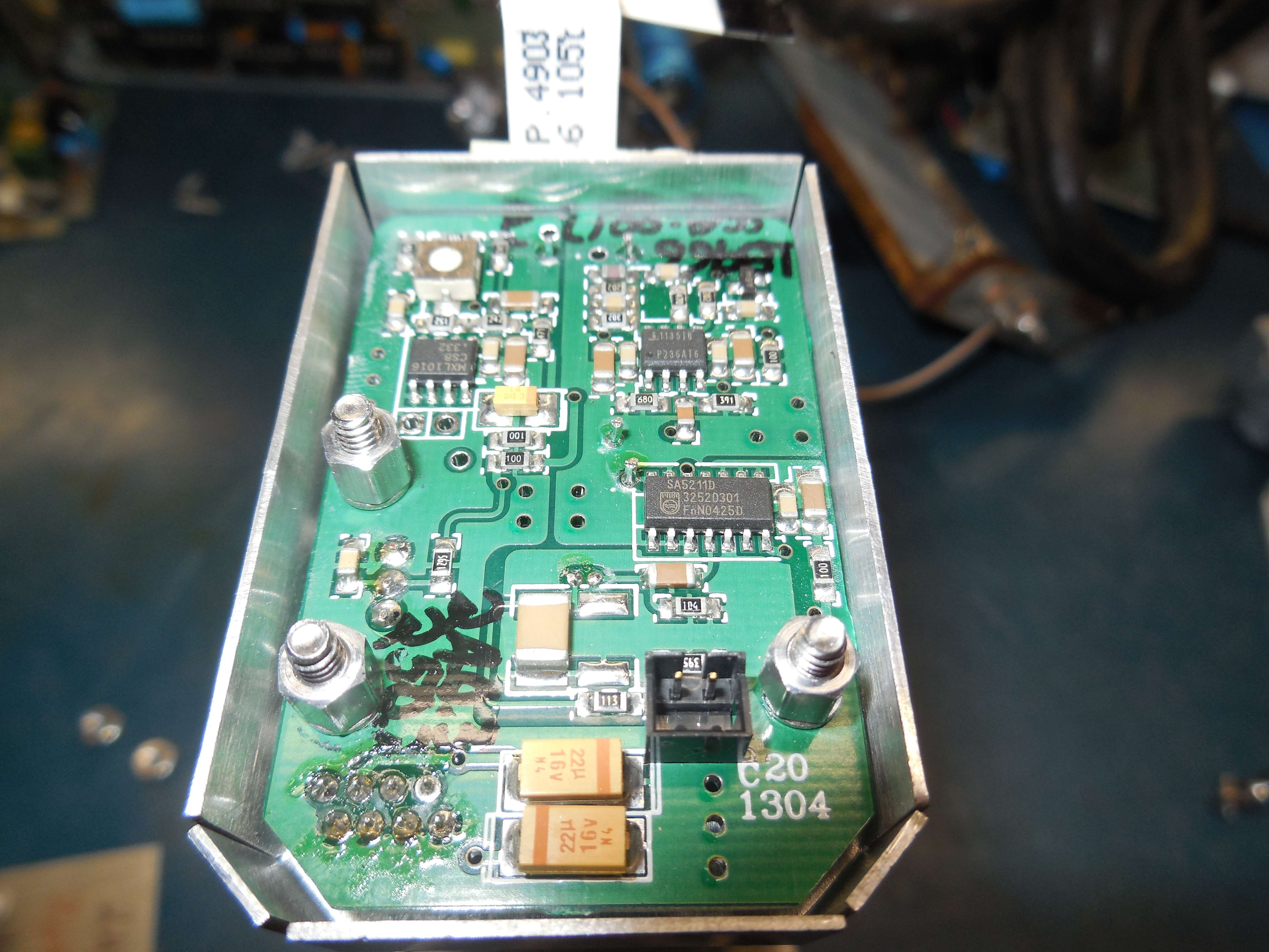
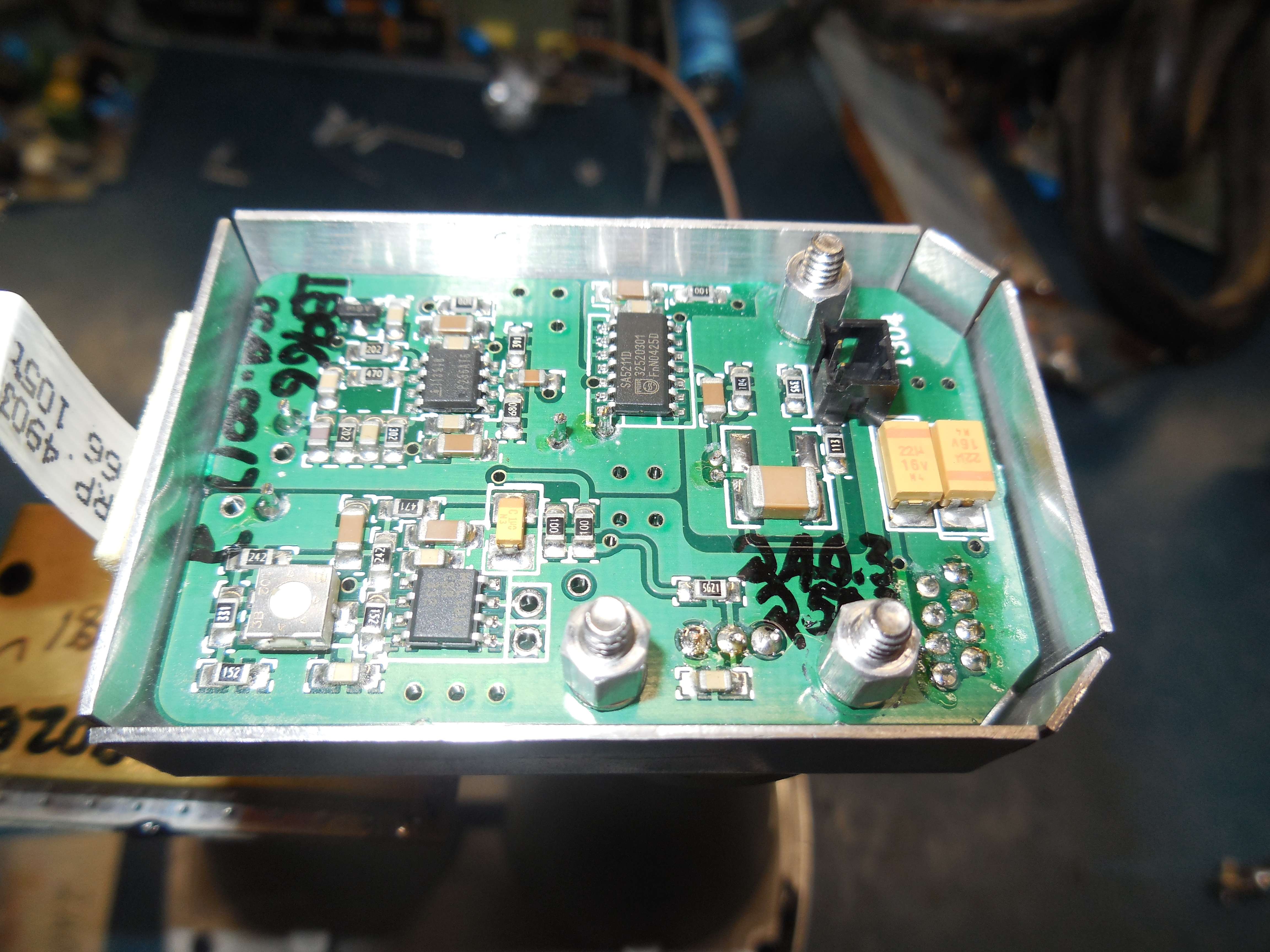
SA5211 transimpedance amplifier.
MXL1016 ultra-fast precision TTL comparator.
I think the Intersil "113518" is a voltage regulator?
PIN Photodiode marked "".
There is a +450 VDC reverse bias on the PIN photodiode.
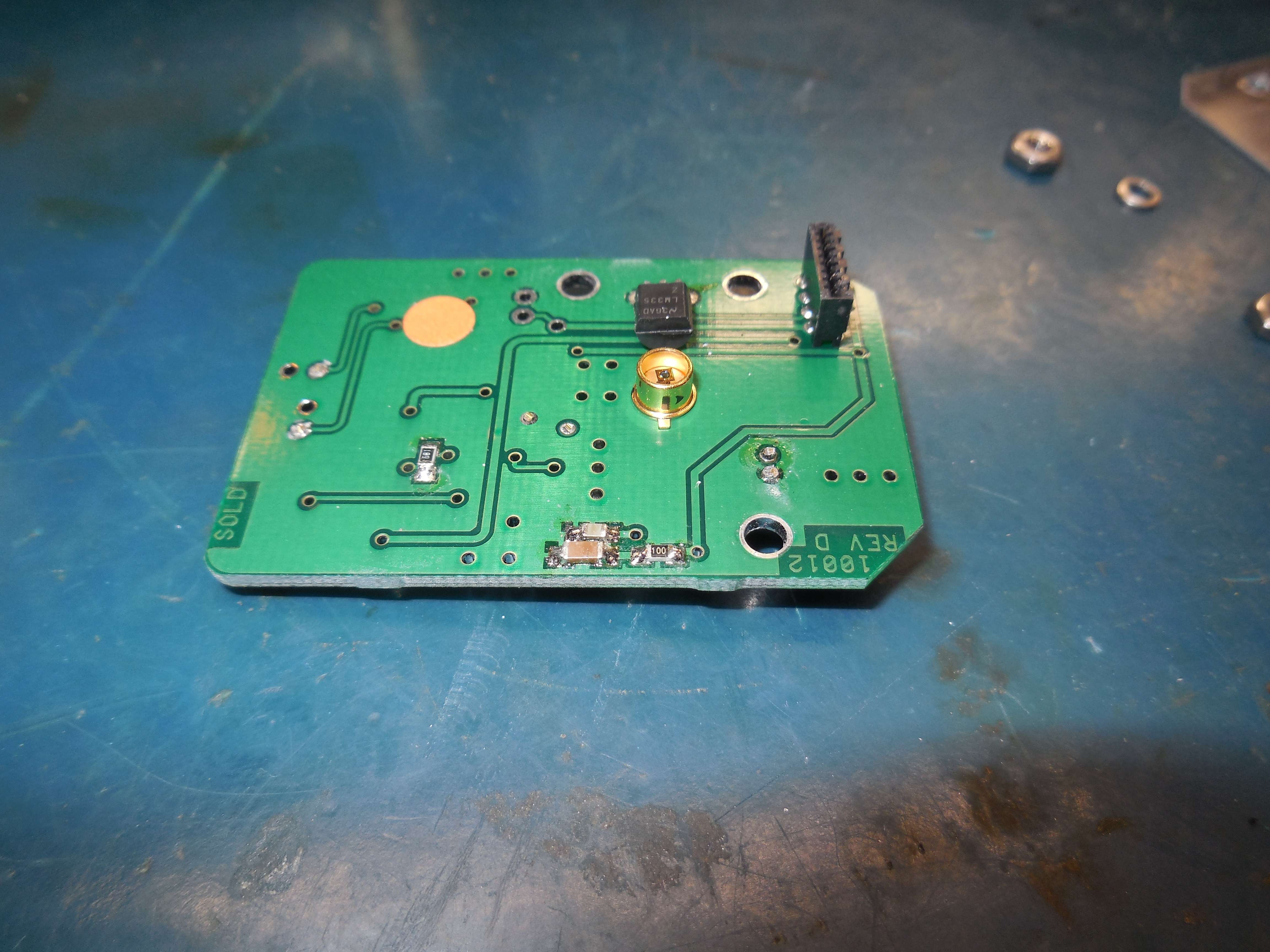
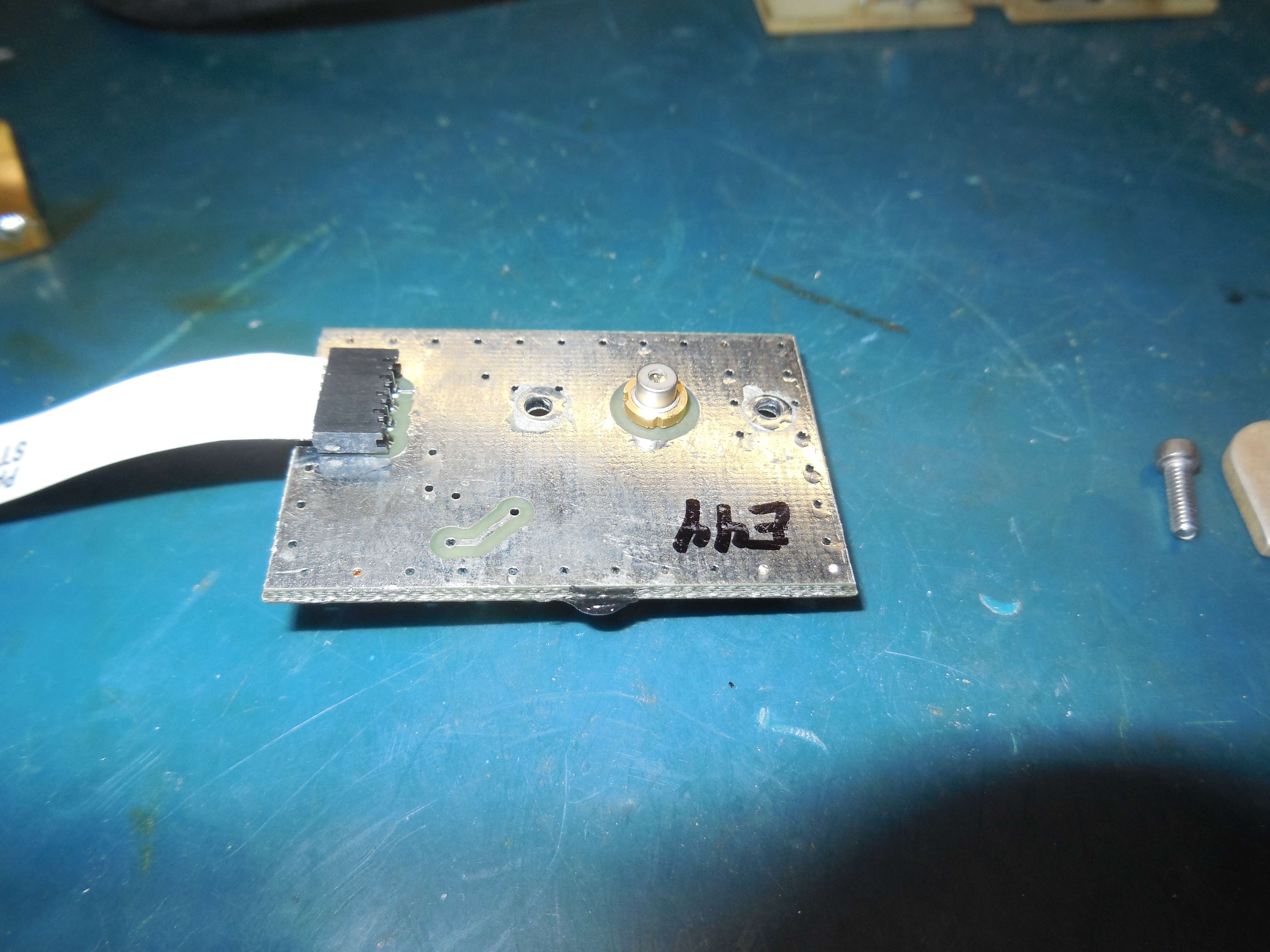
Laser diode board mounted in place.
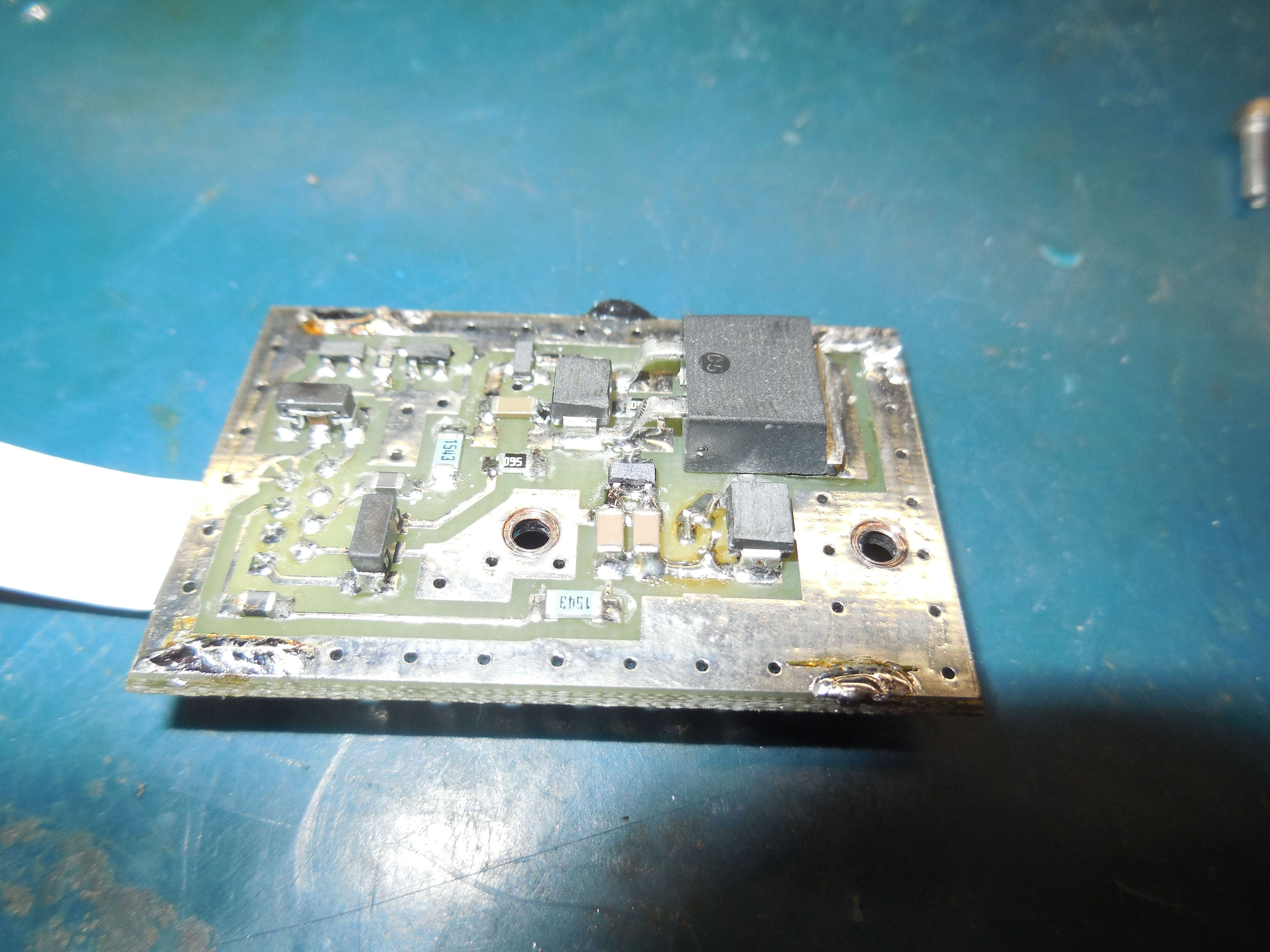
Laser diode board.
ICs and transistors were sanded down. A faint International Rectifier logo was still visible on the large black device, it's probably a MOSFET of some type The middle-sized black devices are diode or Zeners.
The transmit laser diode.
It looks like a regular 10 mW, 5.6 mm infrared laser diode, but since it is "pulsed" (20 nanonsecond or so pulse widths), it is capable of a very high optical output power.
Here is an example of a IR laser diode from ROHM capable of high output power pulses: RLD90QZW8 (Driver Schematic)