This is a collection of notes and experiments with low-cost MicroSource MSS252-791-002 synthesized YIG oscillator modules you can find on eBay or at ham radio swapfests.
It doesn't have best phase noise (or tuning steps), but it's very easy to work with and program. No external microcontroller, just a 960 MHz reference input and standard +/- 15 VDC and +5 VDC power supplies.
The initial data came from John Miles, KE5FX.
MicroSource MSS252-791-000 Synthesizer Module Programming Calculator Simple Perl script to calculate M & A values based on pre-doubler YTO frequency and using a 960 MHz reference.
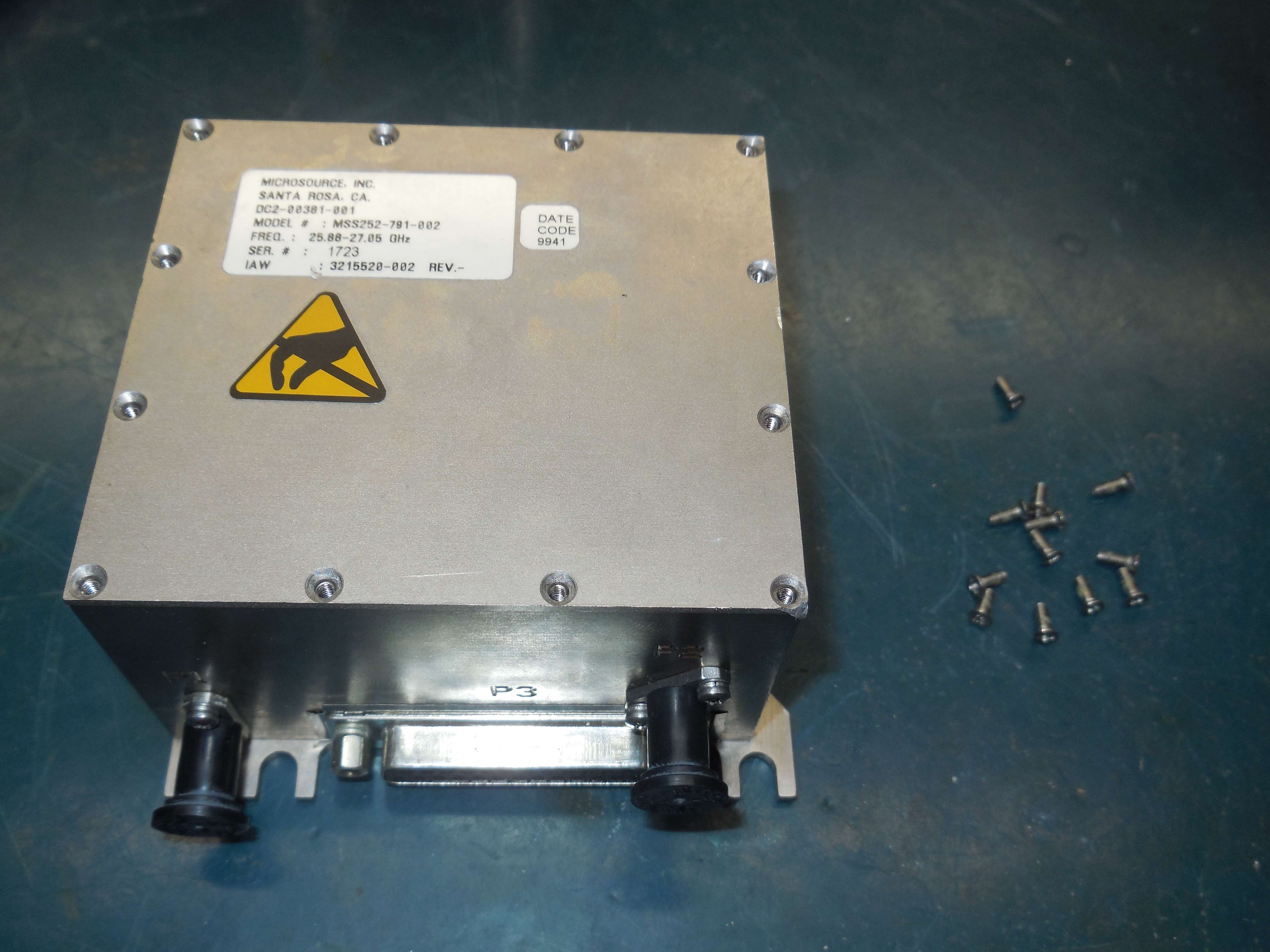
Overview.
Label says:
MICROSOURCE, INC. SANTA ROSE, CA. DC2-00381-001 MODEL # : MSS252-791-002 FREQ. : 25.88-27.05 GHz SER. # : 1723 IAW : 3215520-002 REV.- DATE CODE 9941 |
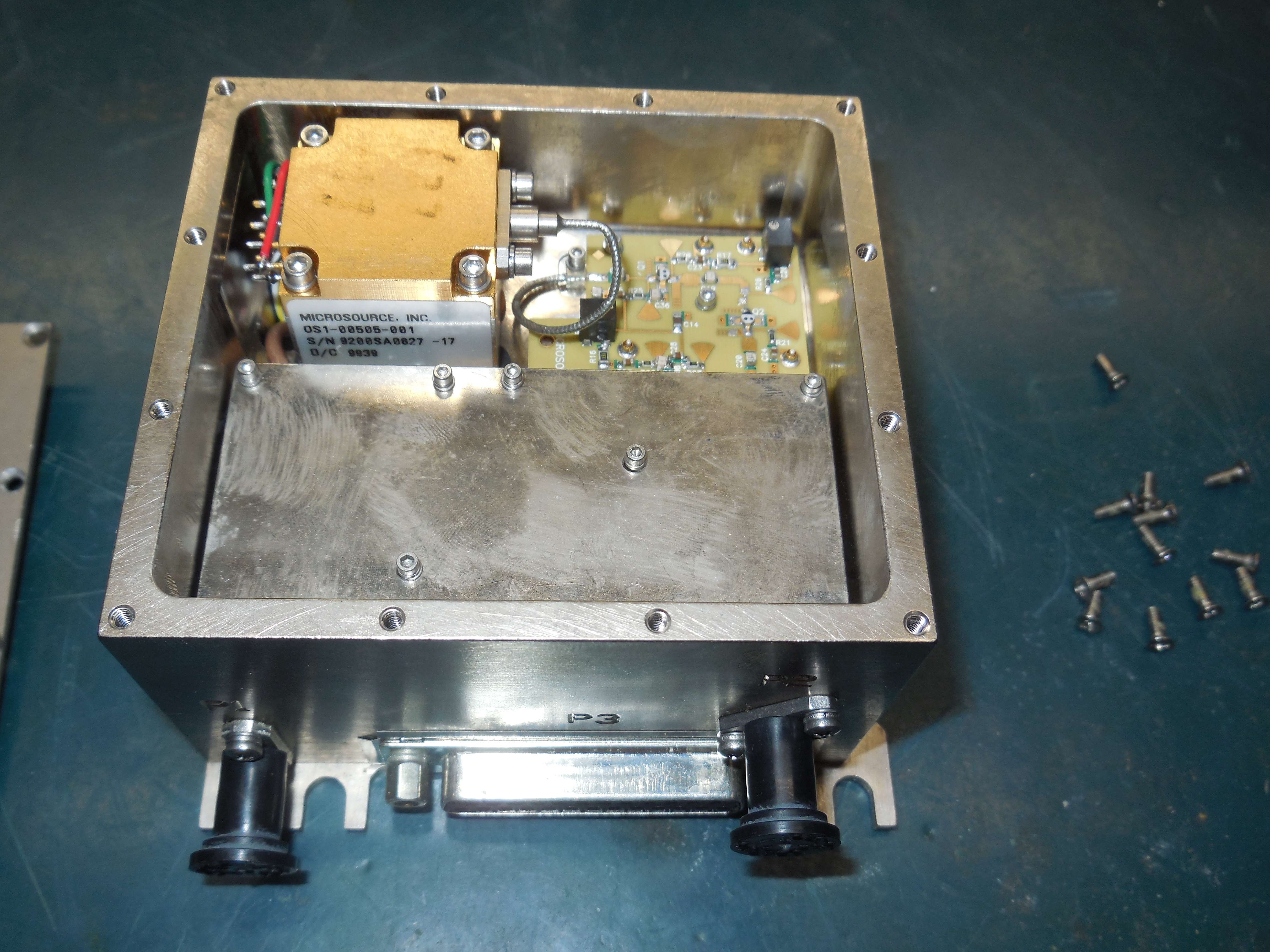
Removing the top cover. It is very well made.
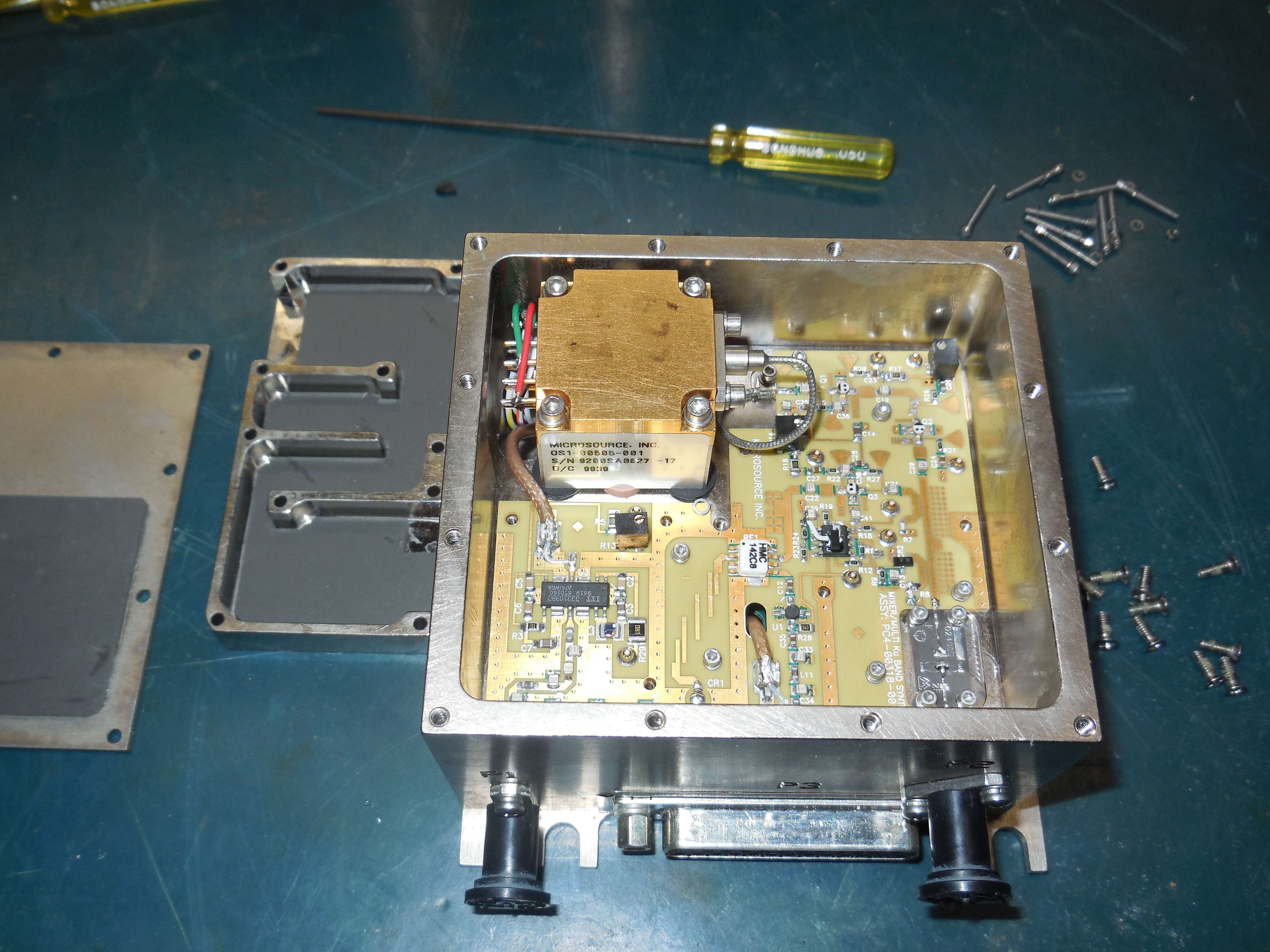
Removing the internal RF cover.
The 12-14 GHz YIG-tuned oscillator (YTO) is the large gold cube on the upper-left.
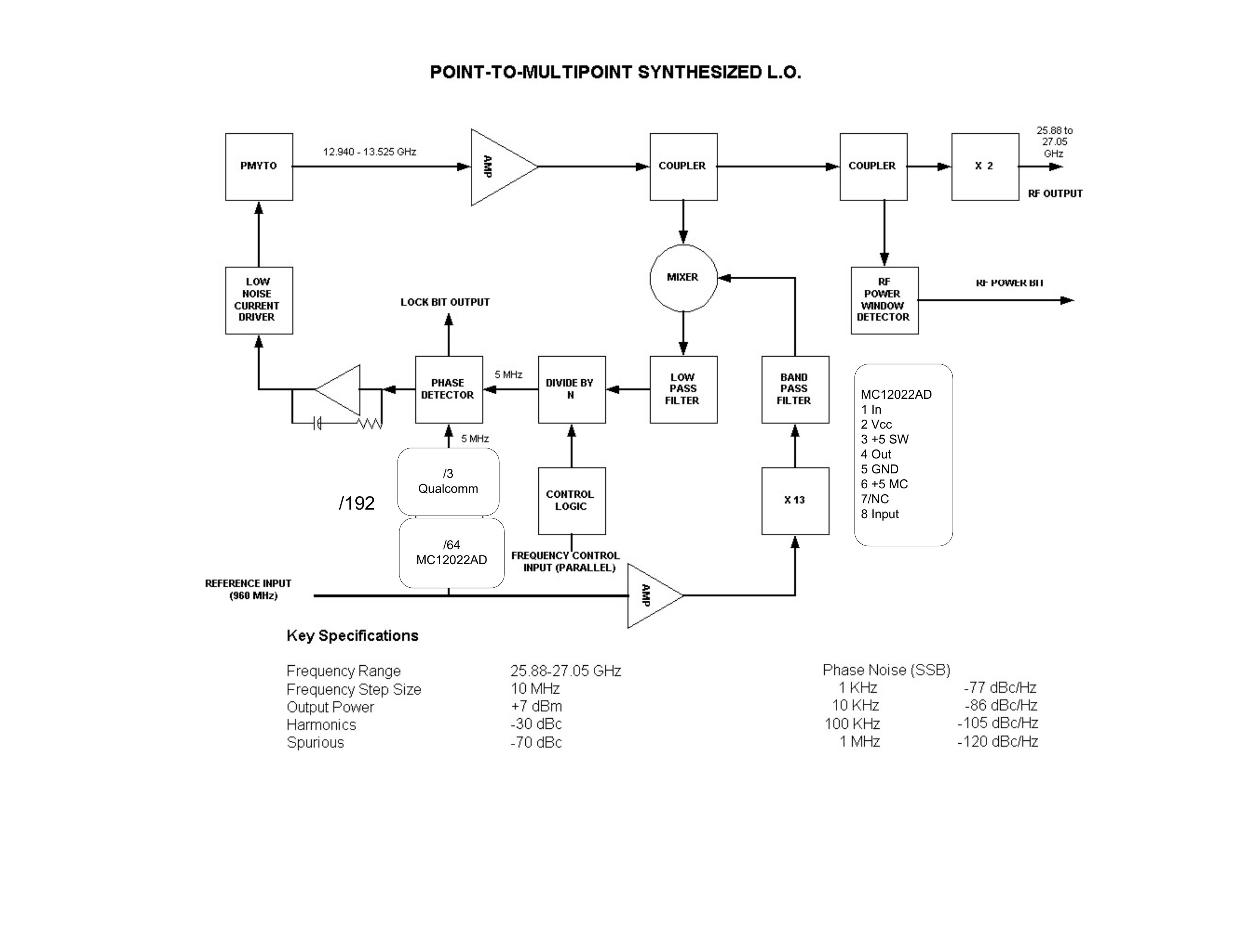
the YTO feeds a series of amplifiers and couplers, where one RF signal is downconverted to 5 MHz reference, and the other is doubled to around 26 GHz for the final RF output.
The label on the YTO reads:
MICROSOURCE, INC. OS1-00505-001 S/N 9200SA0627-17 D/C 9939 |
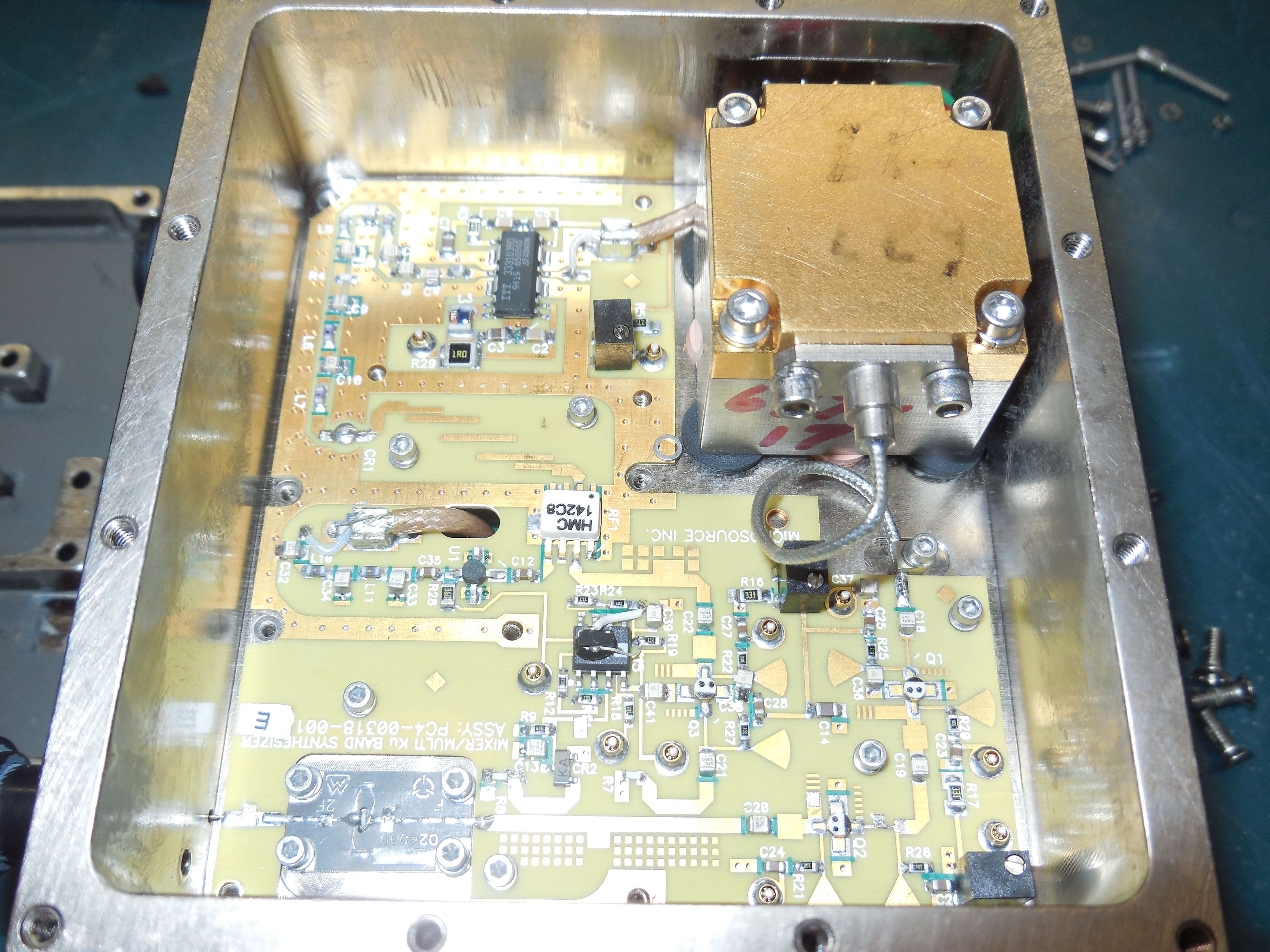
Alternate view.
The reference mixer is a Hittite HMC142. This passive mixer is good up to 18 GHz.
The diode epoxied on the op-amp is for a temperature-compensated RF detector fed by the microstripline coupler just below it.
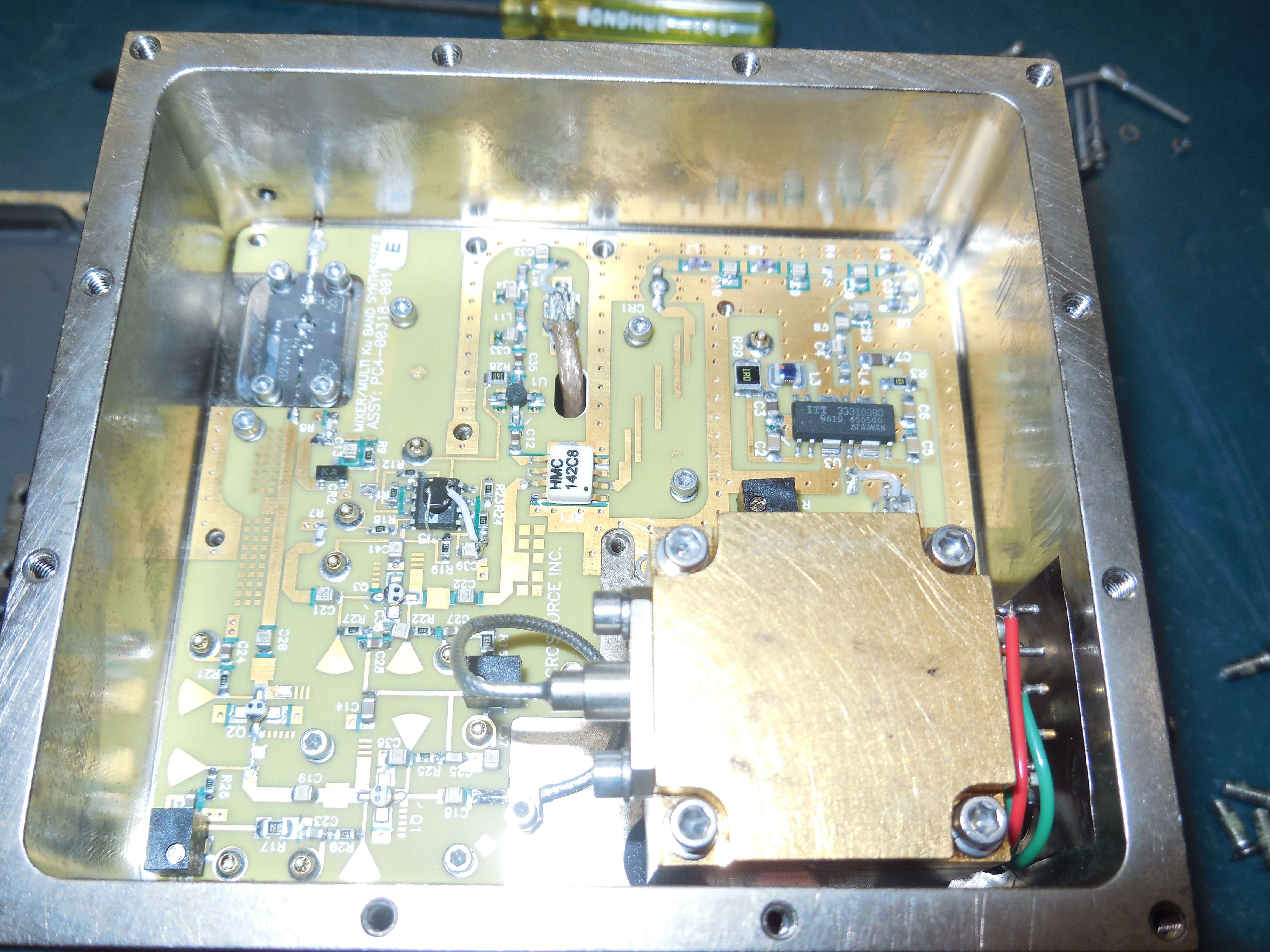
Alternate view.
The ITT device is a 960 MHz amplifier of some sort to drive the x13 diode multiplier.
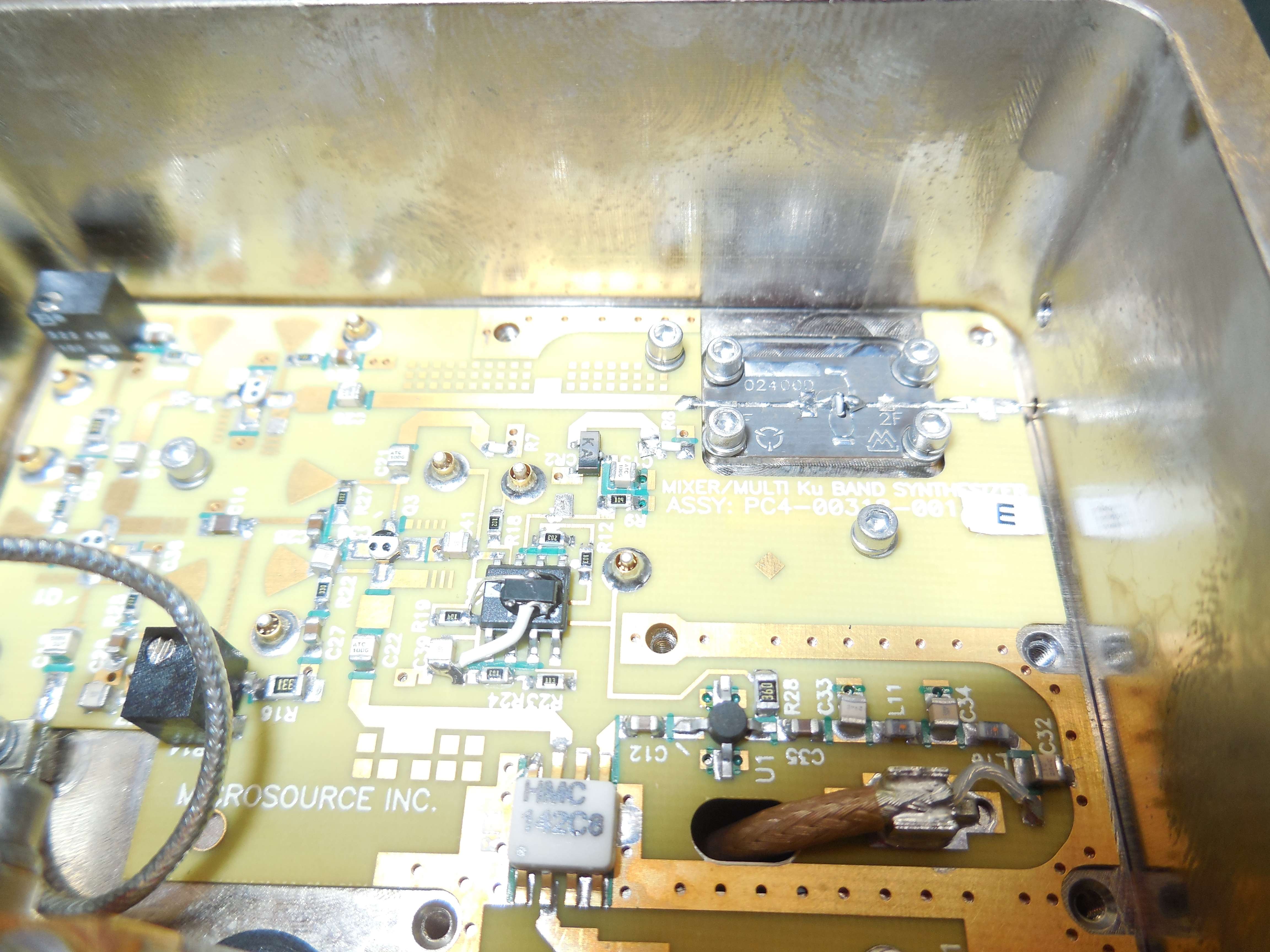
Passive frequency doubler from Marki Microwave.
The frequency doubler can be removed and bypassed with a short piece of conformable coax.
The SMA RF output connector (P2) should also be replaced with a SMA-K version, but that is optional.
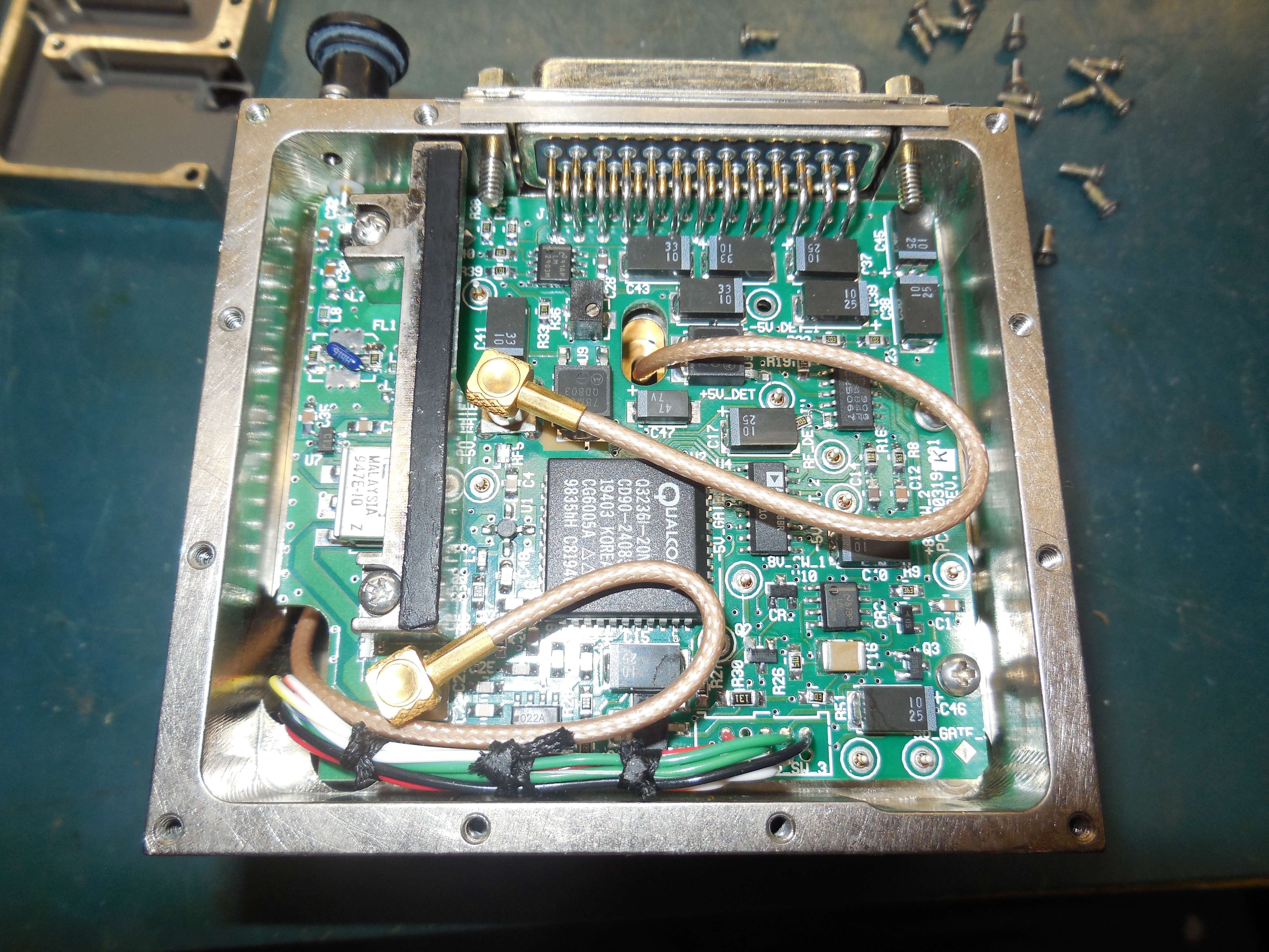
PLL synthesizer section cover removed.
It's based around a Qualcomm Q3236 and a Motorola MC12022 prescaler.
The 960 MHz reference input (P1) is divided by 64 with the MC12022 and then divided by 3 in the Q3236 for total division of 192. That turns the 960 MHz reference input to an internal 5 MHz reference for the PLL itself.
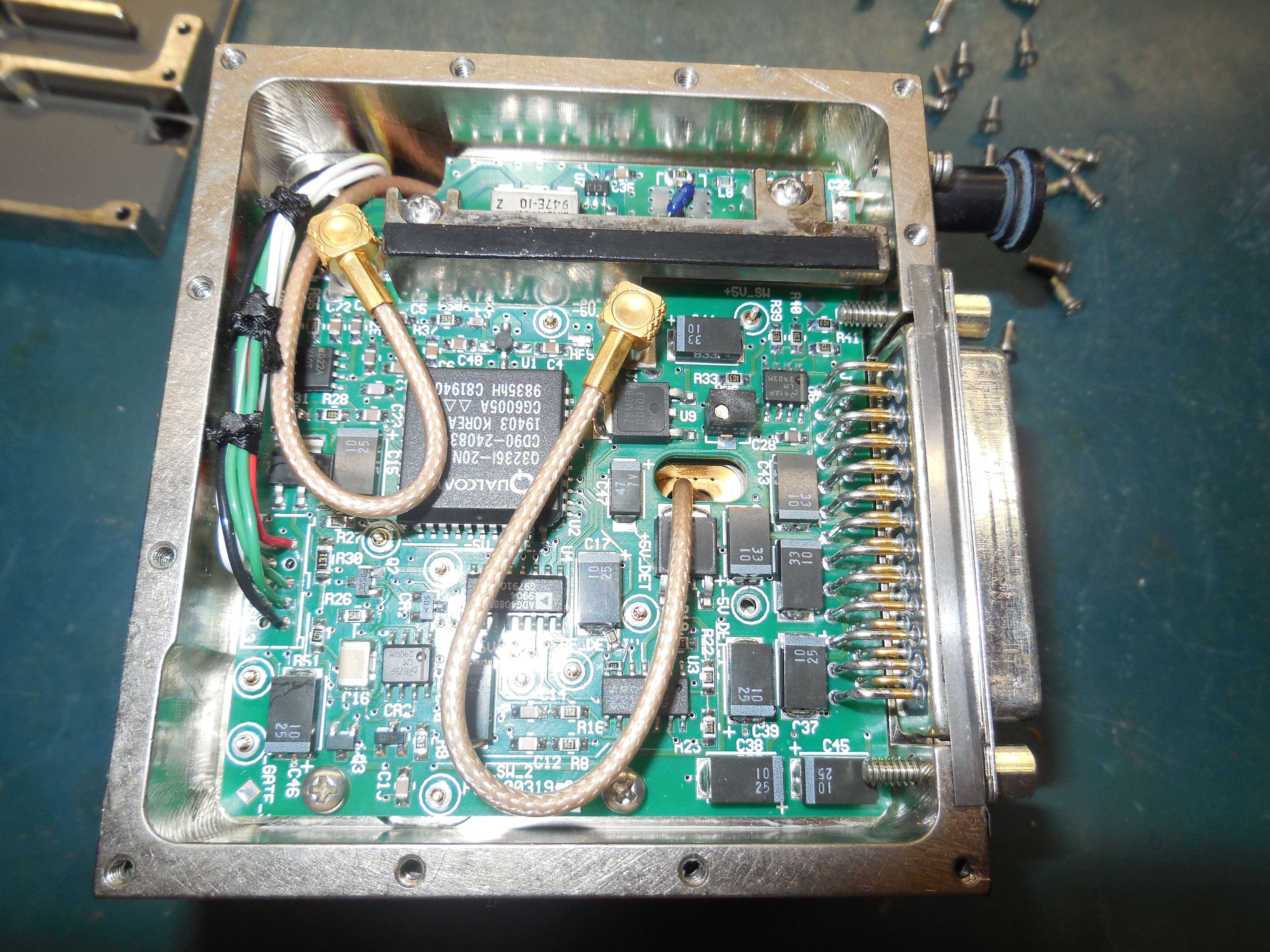
Alternate view.
The Qualcomm Q3236 is parallel-programmed (9-bits) via the DB-25 connector (P3).
Tie a pin to +5V for a logic "1" and ground it for a logic "0".
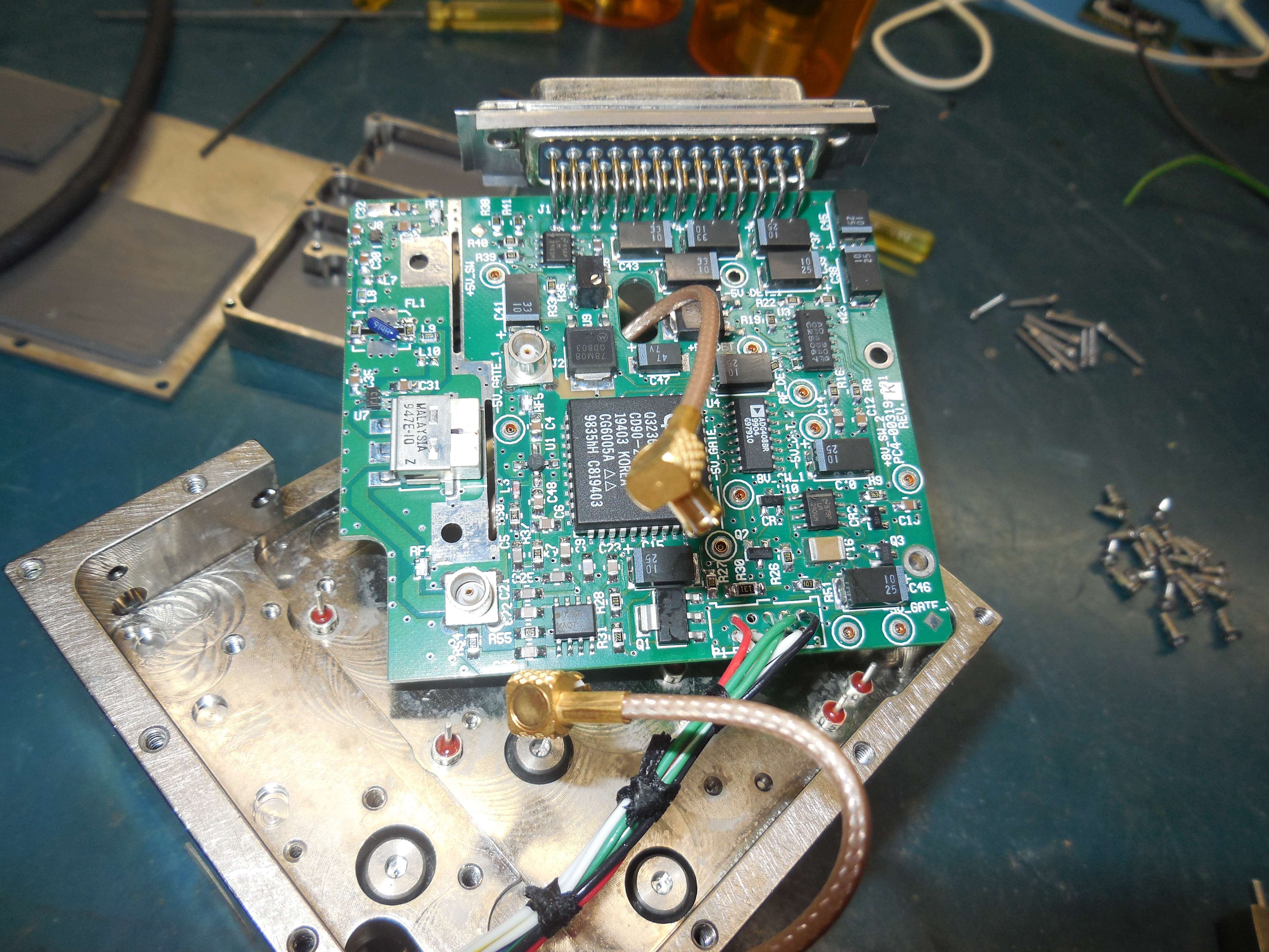
Alternate view with the board removed.
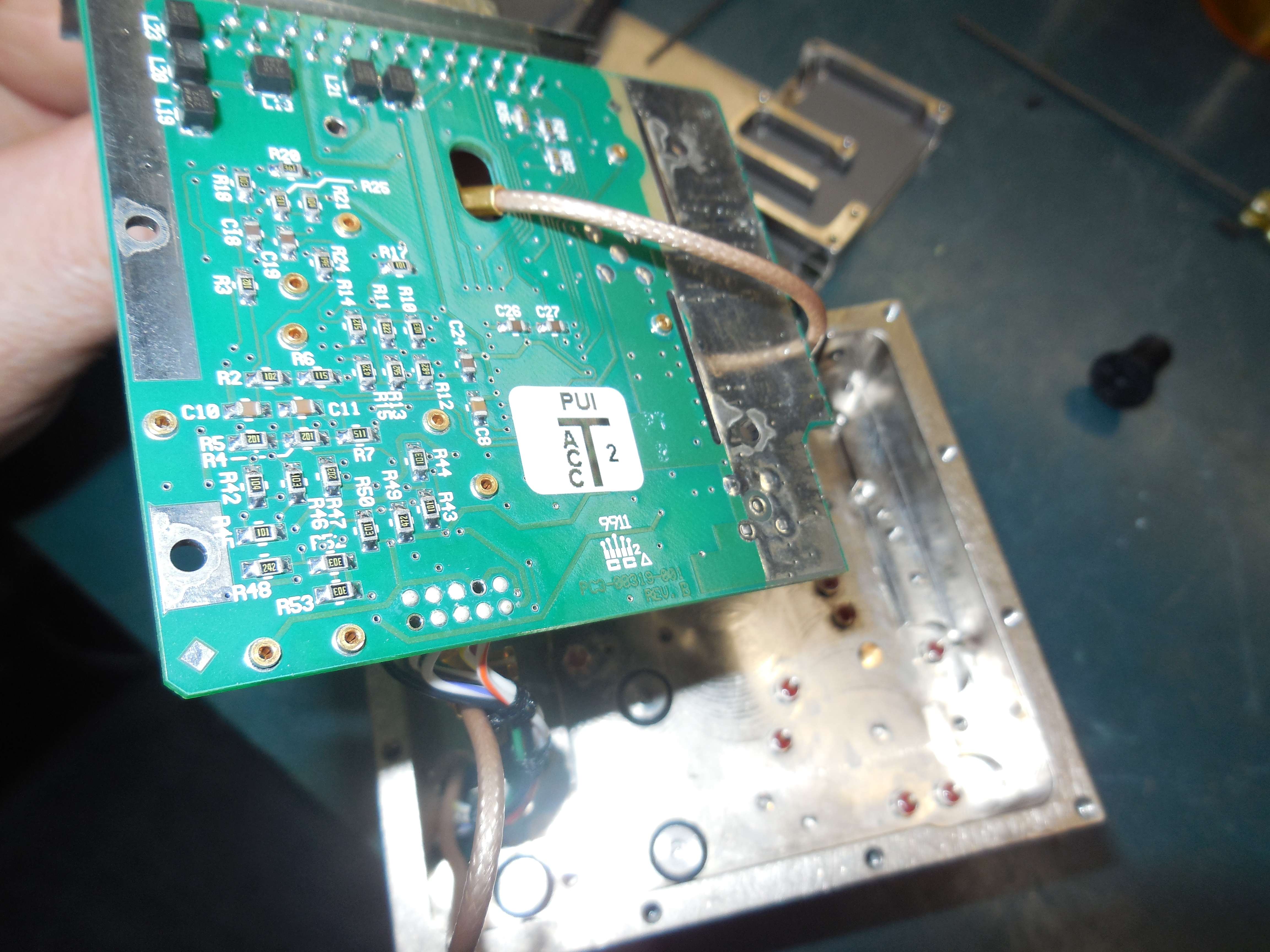
Bottom view.
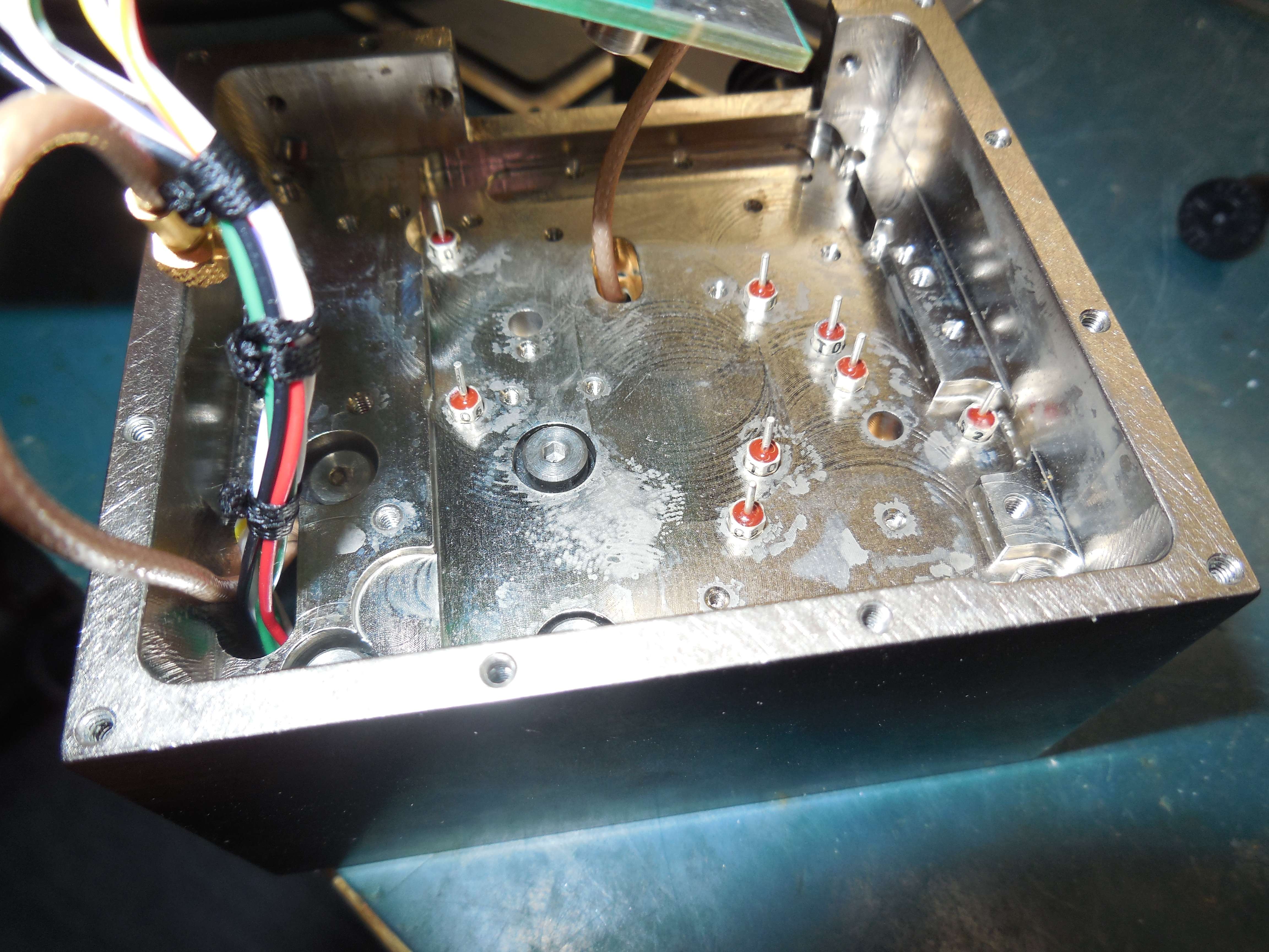
Very nice feed-through capacitor connections.
P3 Connection Data
DB-25 Reference Q3236 Function 01 D3 A3 02 D1 A1 03 D8 M4 04 D6 M2 05 D4 M0 06 PLL Lock 07 RF Power Bit 08 +5 VDC @ 700 mA 09 +15 VDC @ 300 mA 10 -15 VDC @ 45 mA 11 No Connection 12 No Connection 13 No Connection 14 D2 A2 15 D0 A0 16 D7 M3 17 D5 M1 18 Ground 19 Ground 20 Ground 21 Ground 22 Ground 23 Ground 24 No Connection 25 No Connection |
Programming Notes
Calculate: N = Fmix / Fpfd where Fpfd is always 5 MHz (960 MHz / 192) and Fmix is the desired YTO frequency Fyto minus 12480 MHz (960 * 13). Then, calculate M and A: M = int(N/10) - 1 A = N - 10(M + 1) where the lower 5-bits of M are applied to these DB-25 pins: M0: Pin 5 M1: Pin 17 M2: Pin 4 M3: Pin 16 M4: Pin 3 and A is a 4-bit value applied to these DB-25 pins: A0: Pin 15 A1: Pin 2 A2: Pin 14 A3: Pin 1 Example: For YTO of 13000 MHz (26 GHz output): N: 104 M: 9 (01001 in 5-bit binary) A: 4 ( 0100 in 4-bit binary M0: Logic 1 (Tie to +5V) M1: Logic 0 (Tie to Ground) M2: Logic 0 M3: Logic 1 M4: Logic 0 A0: Logic 0 A1: Logic 0 A2: Logic 1 A3: Logic 0 Notes: * Register value constraints: A <= M + 1, M = [1-31], N = [90-1295] * Consequently, supported values of N range from 90 (M = 8, A = 0, Fyto = 12930 MHz) to 329 (M = 31, A = 9, Fyto = 14125 MHz) * Qualcomm Q3236 PLL chip modes are direct-parallel input with legacy Q3036 behavior. * Final output frequency will be 2 * Fyto MHz unless you remove the doubler. |
Or using the provided Perl script:
$ ./microsource.pl 13000

MicroSource MSS252-791-000 Synthesizer Module Programming Calculator

   REF: 960.000000 MHz
  Fpfd: 5.000000 MHz
  Fyto: 13000.0000 MHz
      : 26000.0000 MHz  (With internal doubler)
     N: 104    (N = 90-1295, but the YTO only tunes N = 90-329)
     M: 9   (M = 1-31)
     A: 4   (A <= 10)

The lower 5-bits of M (9) are applied to these DB-25 pins:
 M0 : Pin 5
 M1 : Pin 17
 M2 : Pin 4
 M3 : Pin 16
 M4 : Pin 3

MMMMM
43210
|||||     (Where 0 is ground and 1 is +5V)
01001

The lower 4-bits of A (4) are applied to these DB-25 pins:
 A0 : Pin 15
 A1 : Pin 2
 A2 : Pin 14
 A3 : Pin 1

AAAA
3210
||||     (Where 0 is ground and 1 is +5V)
0100

Other DB-25 pins:
 Pin 6 : F LOCK
 Pin 7 : PWR BIT
 Pin 8 : +5 VDC @ 700 mA
 Pin 9 : +15 VDC @ 300 mA
Pin 10 : -15 VDC @ 45 mA
Pins 18-23 : Ground
|