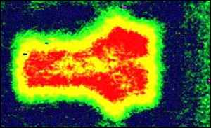
 Electrons are forced through a tiny
gate Electrons are forced through a tiny
gate |
By BBC News Online Science Editor Dr David Whitehouse
Scientists have produced the world's smallest transistor.
This new design may allow silicon chips to continue to get smaller. It could also double the processing speeds of some chips.
The 50-nanometer transistor - roughly 1/2000 the width of a human hair - is known as a "vertical" transistor because all of its components are built on top of a silicon wafer.
Another key difference is that a conventional transistor has only one "gate," which switches current on and off.
The vertical transistor, however, resembles a rectangular block with a "gate" on two sides. This means that the vertical transistor could nearly double the processing speeds of some silicon chips.
Brick wall
"Our vertical transistor eventually could supersede the conventional transistor, which many experts in the semiconductor industry anticipate will hit a brick wall within the next 10 years," said Bell Labs researcher Jack Hergenrother.
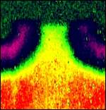
 Smaller gates could mean faster
chips Smaller gates could mean faster
chips |
Light is used to etch patterns on silicon chips.
However, as transistors continue to shrink in size, light will be unable
to produce the smaller features required.
The vertical transistor may solve this problem by using the thickness of a precisely-controlled layer of material, rather than light, to set the gate size.
"Suppose you have a can of paint and a big paintbrush, and you are asked to paint the thinnest possible line," Hergenrother said. "If you just tried to paint the line freehand, that would be similar to the light approach.
"However, if you paint a flat surface, cut it vertically and look at it on edge, you will see a line that's as thin as the layer of paint. A similar principle is used in our transistor to produce the smallest gates ever made with the control that industry requires."
Insulating layer
The vertical transistor design also may help forestall another challenge faced when making smaller transistors: the ever shrinking insulating layer.
This layer lies between the transistor's gate and the channel through which current flows, thus preventing a short circuit. In recent years the insulating layers have shrunk dramatically to increase the amount of current that transistors can carry.
However, these layers will soon be so thin that electrons can leak through them, which wastes power and causes the chips to fail. Many scientists believe that this will be the end of the conventional transistor.
Industry is trying to find alternative materials for the insulating layer, instead of today's silicon dioxide. A major problem is that most potential replacements are sensitive to the high temperatures used in the semiconductor manufacturing process.
The vertical transistor approach eliminates this problem because the gate and insulating layer are applied last in the manufacturing process, after all the high-temperature steps are completed.
The transistor was invented by three scientists at the Bell Laboratories in 1947.
Orginial Source
All logos and trademarks in this site are property of their respective owner. FAIR USE NOTICE: This site contains copyrighted material the use of which has not always been specifically authorized by the copyright owner. We are making such material available in our efforts to advance understanding of environmental, political, human rights, economic, democracy, scientific, and social justice issues, and for the general purpose of criticism, comment, news reporting, teaching, research and / or educational purposes only. We believe this constitutes a 'fair use' of any such copyrighted material as provided for in section 107 of the US Copyright Law. In accordance with Title 17 U.S.C. Section 107, the material on this site is distributed without profit to those who have expressed a prior interest in receiving the included information for research and educational purposes. If you wish to use this material for purposes other than provided by law. You must obtain permission from the copyright owner. For more information go to: http://fairuse.stanford.edu/Copyright_and_Fair_Use_Overview/chapter9/index.html,