Scotty's Spectrum Analyzer - Control Board
Overview
This is my version of the control board for Scotty Sprowls' Modularized Spectrum Analyzer (MSA) project. The original MSA control board design is SLIM-CB-NV.
There are no major differences between my version and the Scotty version, except for adding ferrite beads on the incoming DB25 data lines.
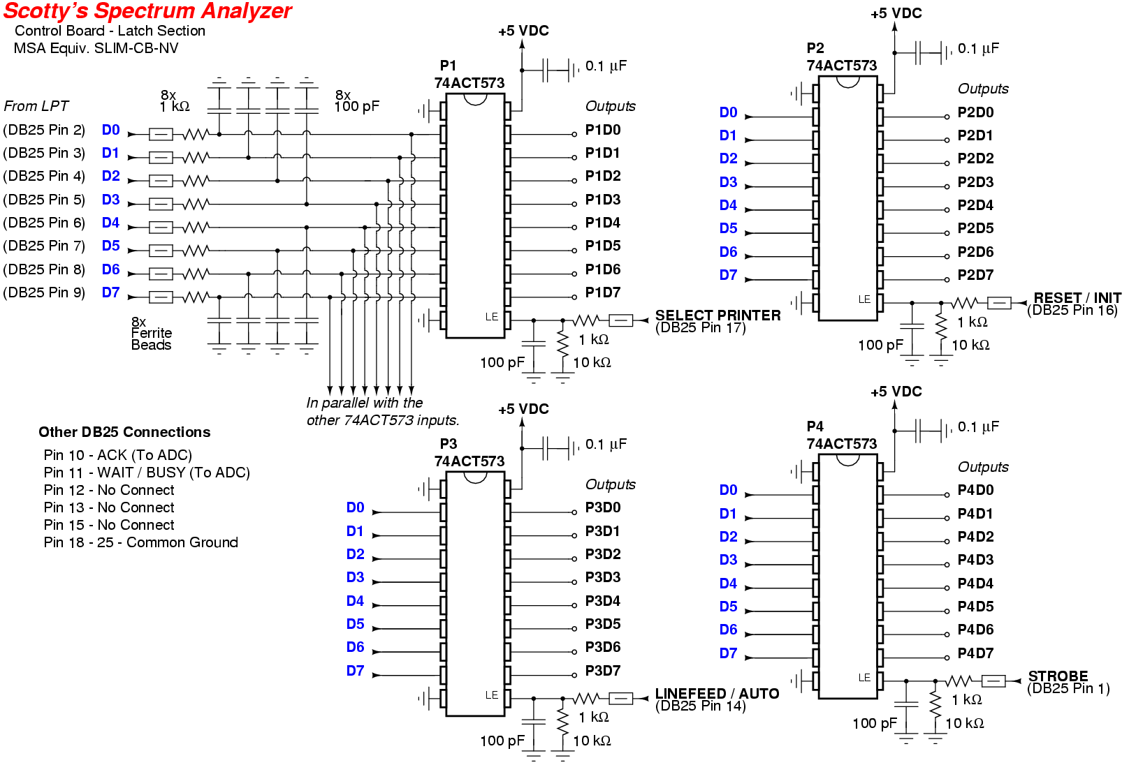
The latch section of the control board consists of four 74ACT573 buffer latches with CMOS outputs and TTL compatible inputs The inputs are from the computer's standard LPT printer port, carried via a DB25 female connector and matching double-male DB25 cable. Try to keep the cable length as short as possible.
The outputs of the latches are accessible via four 9-pin SIP sockets used as headers. These are optional, but recommended to help in troubleshooting.
Another 4-pin header is a direct connection for the four LPT status signals which are "read" by the computer. Two of these signals, ACK (pin 10) and WAIT (pin 11), are used by the MSA's A-to-D converter. Note that the WAIT line is often referred to as the BUSY line. The other two status lines, PE (pin 12 - Paper End or Paper Out) and SELECT (pin 13) are not used by the MSA or VNA, but may be in the future.
The four status signals should have 2.2 kohm pull-up resistors (to +5V). Some home computers do not have internal pull-up resistors and, if so, these resistors are necessary. Here is a test to see if the pull-up resistors are required. Re-boot the computer, the use a voltmeter to measure from computer ground to LPT port pins 10, 11, 12, and 13. If any of these pins are showing greater than +2.0 volts, the pull-ups are not required.
All four of the 74ACT573 latch ICs are fed by the parallel data from the computer. The data will be passed to the latch's output when its "latch enable" line is commanded high. If enable is kept high, the output data will follow the input data. When the enable is brought low, the data will be retained as a latch.
The control board is a generic module that will be integrated into a higher assembly. Therefore, the signal names in the schematic are generic. For example, the data signal that exits the computer is called D0. It is buffered by the four 74ACT573 latches, labeled P1-P4. The name changes at the output of each latch, for example, P1D0. This is Data Bit 0 on connector P1 (P1 output). Once the control board is integrated into a higher assembly, the signals are assigned more meaningful names.
The control board is the only module which doesn't require shielding or a proper circuit board. The control board shown here was made using a perf board from Radio Shack (276-147). The 74ACT573s should be in sockets to ease replacement in case of damage from static or anything else. The wiring on the perf board can be done using point-to-point solder "blobs" and tinned buss wire.
Not all the signals will be used when just building the spectrum analyzer, but they all should be noted in case you want to expand on the design or build the matching Vector Network Analyzer (VNA) or tracking generator in the future.
Control Board - Latch Section Wiring Diagram
Latch Output          Module Signal

P1D0                  CLK for PLO1, PLO2, PLO3, DDS1 (WCLK), DDS3 (WCLK)
P1D1                  DATA for PLO1
P1D2                  BD7 for DDS1
P1D3                  DATA for PLO3 (not used)
P1D4                  DATA for PLO2, BD7 for DDS3
P1D5                  A0 for Filter Bank (not used)
P1D6                  A1 for Filter Bank (not used)
P1D7                  Not used

P2D0                  LE for PLO1
P2D1                  FQUD for DDS1
P2D2                  LE for PLO3 (not used)
P2D3                  FQUD for DDS3 (not used)
P2D4                  LE for PLO2
P2D5                  Reserved PDM (not used)
P2D6                  INVP for PDM (not used)
P2D7                  Not used

P3D0                  Not used
P3D1                  Not used
P3D2                  Not used
P3D3                  Not used
P3D4                  Not used
P3D5                  Not used
P3D6                  SERCLK for ADC
P3D7                  CONVERT for ADC

P4D0                  V0 for Video Filter (not used)
P4D1                  V1 for Video Filter (not used)
P4D2                  G0 for RF Path Switch (not used)
P4D3                  G1 for RF Path Switch (not used)
P4D4                  FR for DUT Switch (not used)
P4D5                  TR for VNA Bridge (not used)
P4D6                  Not used
P4D7                  PULSE for DUT or RF Path Switch (not used)
Pictures & Construction Notes
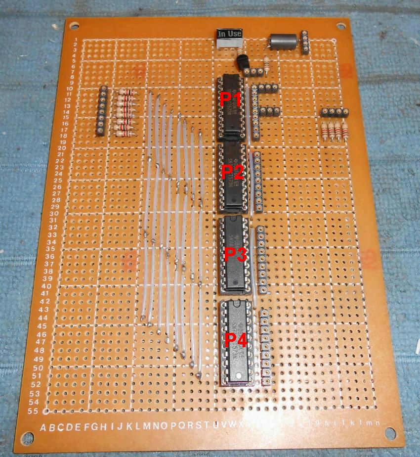
Overview of the control board built on a piece of Radio Shack perf board.
The 74ACT573 latches should be in 20-pin sockets.
SIP sockets are used as headers for the output connections. This allows both matching with another SIP socket or direct soldered wired connections.
The parallel inputs to the latches are on the left.
The outputs from the latches are on the right.
The 4-pin SIP sockets on the right side is for the latch enable lines.
The 4-pin SIP sockets on the top near the ferrite bead are for the circuit's +12 VDC power input.
The series 1 kohm resistors are used to prevent signal reflections on the parallel cable connection to the computer.
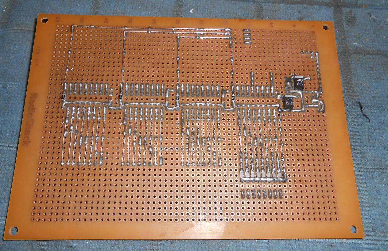
Bottom overview of the control board.
Solder blobs and tinned buss wire are used for all the connections.
The 0.1 inch copper pad spacing on the perf board means you can use 1206 size surface-mount components for the 100 pF capacitor / 10 kohm resistor network on the 74ACT573 latch enable lines and for the 0.1 µF capacitor on the Vcc lines.
There are also surface-mount 100 pF capacitors on the D0 - D7 input lines from the parallel port.
A standard 78L05 voltage regulator with 10 µF caps on the input and output supplies the +5 VDC for the 74ACT573 latches. This is not shown in the schematic.
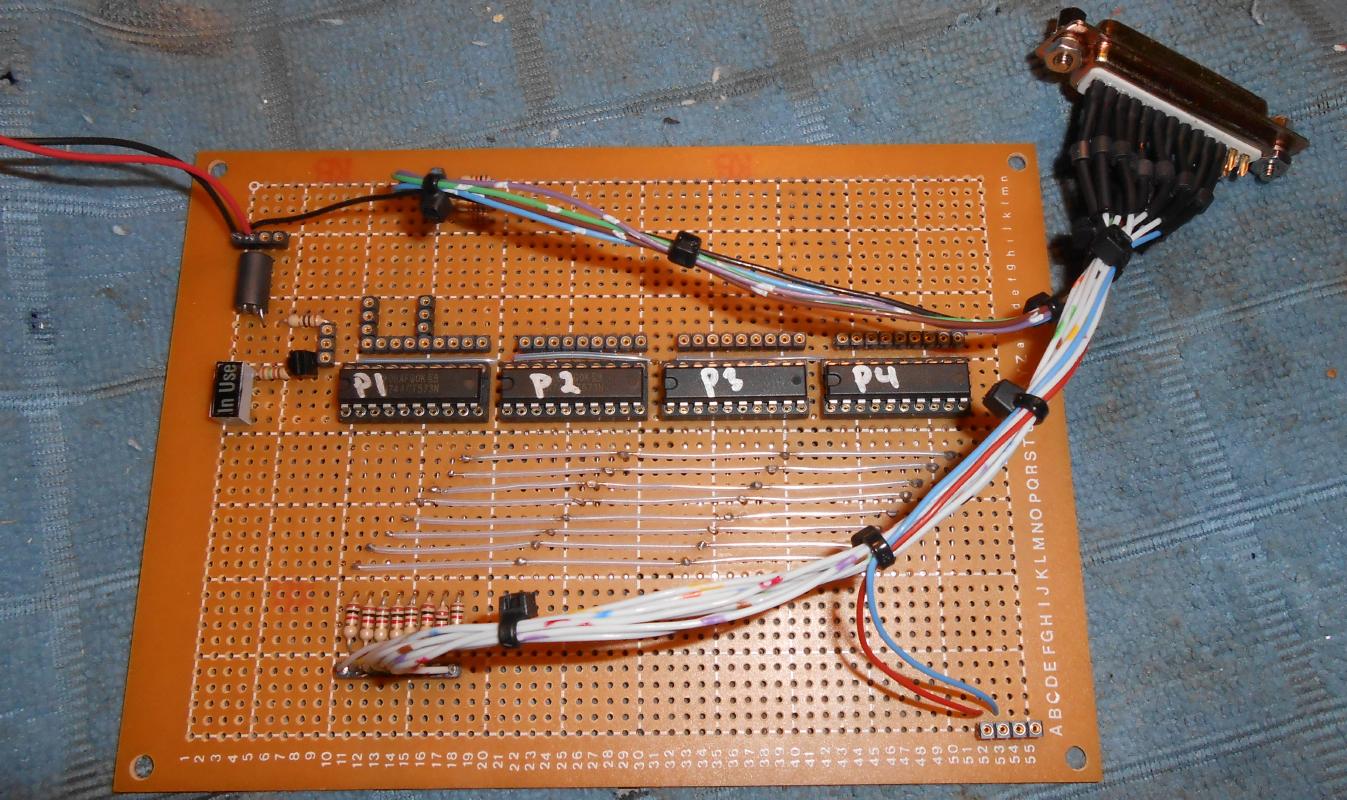
Overview of the completed control board with the DB25 (female) wiring added.
The DB25 wires should be as short as possible.
The wire connections to the outputs of the latches should be in a "star" configuration, that is, tied to a single point.
This is especially important for the P1D0 connection as this serves at the clock signal for a number of modules. Also try to make those interconnection wires all the same length to minimize clock signal reflections.
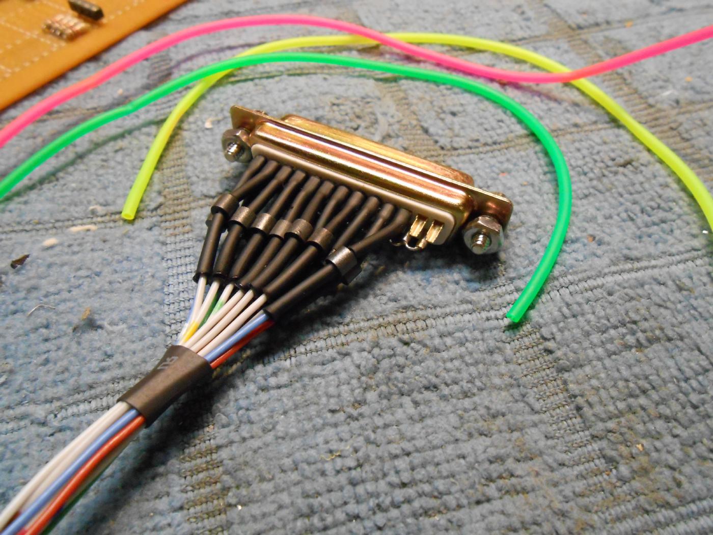
Type 43 ferrite beads were added to each of the data and status lines on the DB25 connector.
"Jelly" bracelet material available at Hobby Lobby is used to isolate each of the solder connections and to secure the ferrite beads.
The common ground wires (pins 18 - 25) should not have a ferrite bead on it.
Schematic
Notes & Links
Return to Constructing Scotty Sprowls' 1 GHz RF Spectrum Analyzer