(AI Assisted)
- Modulated Light DX Receiver Circuitry
- OPTICAL COMMUNICATION FOR THE AMATEUR by Chris Long, originally published in Amateur Radio magazine by the Wireless Institute of Australia, Melbourne, January 1979.
- A Low-Noise PIN Diode Laser Receiver! by K3PGP
- A Comb Filter to Remove AC Hum from Mains-Powered Lighting in an Optical Receiver
- AVR Digital Comb Filter (humnuller) by Dan Stahlke
- PIC Humnuller by Karen Orton
- PIC16F876-04 Ran at 20 MHz
- PIC Files
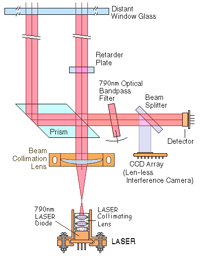
This diagram depicts a homodyne optical interferometric laser microphone (a long-range differential laser vibrometer) designed to remotely detect acoustic vibrations on a distant window glass. Sound waves inside a room cause microscopic vibrations in the window pane, which modulate the optical phase (and path length) of the laser light reflected back from the glass.
1. How the System Works (Stage-by-Stage Analysis)
A. Laser Source & Beam Expander (Bottom)
- 790 nm Laser Diode: Generates near-infrared (NIR) coherent light at 790 nm - just beyond strong human visual sensitivity (appearing at most as a very faint deep-red glow) while remaining well within the peak responsivity range of standard silicon photodiodes and CCDs.
- Laser Collimating Lens & Beam Collimation Lens: Despite the label "Laser Collimating Lens," the ray trace shows this two-element lens focusing the raw diode output to a tight focal waist, after which it diverges into the larger plano-convex beam collimation Lens. Together, these two lenses form a Keplerian beam expander, increasing the beam diameter so that diffraction divergence is minimized over the long distance to the window.
B. Dual-Beam Interferometer Routing (Center & Top)
- Prism (Beam Splitter / Combiner): Intended to split the outgoing beam into two parallel probe beams directed upward toward the window glass, and later recombine the two reflected beams, sending the combined light horizontally to the right toward the detection stage. (Note: There are significant geometric/optical flaws in how this prism is drawn - detailed in Section 2).
- Distant Window Glass: Acts as the vibrating target. Both parallel beams travel across the long gap (indicated by the break lines), reflect off the window glass, and return downward along the same paths.
- Retarder Plate: Placed in only one of the two arms. It introduces a static optical phase shift (or polarization rotation) between the left and right beams. In a homodyne interferometer, this is used to bias the phase difference near the quadrature point (π/2 or 90°), where small acoustic vibrations produce the largest, most linear change in output intensity.
C. Filtering & Detection (Right)
- 790 nm Optical Bandpass Filter: A narrowband interference filter placed in front of the detectors to block ambient sunlight and room lighting. The curved arc and arrow at the bottom indicate it is tilt-tunable—tilting an interference filter shifts its passband center toward slightly shorter wavelengths, allowing fine-tuning to the exact emission wavelength of the laser diode
- Beam Splitter: Splits the returning interference beam into two paths:
- Detector (Right): A single-element photodiode (or phototransistor) converts the time-varying optical interference intensity into an electrical audio signal.
- CCD Array ("Len-less [Lens-less] Interference Camera"): Captures the raw spatial interference fringe pattern across the beam cross-section. Because 790 nm is nearly invisible and aligning two beams over a long distance is difficult, this camera provides real-time visual feedback of beam overlap, tilt, and fringe spacing.
2. Critical Optical & Geometric Flaws in the Diagram
If built strictly as drawn, several components would violate basic optical physics:
The "prism" geometry violates Snell's law and Total Internal Reflection (TIR):
- Exit Face Failure: The horizontal beam inside the glass prism strikes the right-slanted face (tilted at 45°) from the inside. For standard optical glass (n ≈ 1.5), the critical angle for TIR is ≈41.8°. Because 45° > 41.8°, the horizontal beam would undergo total internal reflection straight downward rather than exiting horizontally toward the bandpass filter!
- Outgoing Split Failure: Even if the right-slanted face were coated as a 50/50 beamsplitter (with a mating right-angle prism cemented on to form a flat exit face), an upward-traveling beam reflecting left off a \-sloped face would then hit the \-sloped left face and reflect downward, not upward toward the window. For the prism to send both beams upward and recombine both downward reflections to the right, the left reflecting face would need to be sloped the opposite way (/), and a second prism block would be required on the right to form a proper cube beamsplitter + lateral prism (or a Jamin / Mach-Zehnder assembly).
Backwards plano-convex lens orientation:
- The Beam Collimation Lens is drawn with its flat side facing the collimated beam and its curved side facing the focal point. To minimize spherical aberration, a plano-convex lens should always have its curved side facing the collimated (infinite-conjugate) side and its flat side facing the focal waist.
Missing focusing lens at the detector:
- A wide collimated beam is shown hitting a small photodiode directly. Without a focusing lens in front of the detector, most of the returning optical power misses the active area (or forces the use of a large-area, high-capacitance, noisy photodiode).
Missing polarizer (analyzer) if using polarization phase bias:
- If the Retarder Plate alters polarization (e.g., a λ/4 plate double-passed to rotate polarization by 90°), the two beams become orthogonally polarized and cannot interfere at the detector unless a linear polarizer (analyzer) oriented at 45° is placed before the bandpass filter.
3. Recommended Engineering Improvements
Optical and alignment upgrades:
- Replace the Prism with a Proper Polarizing Interferometer / Mach-Zehnder Block: Use a precision beamsplitter cube paired with a 45° right-angle prism (or mirror) to eliminate internal reflection errors and stray ghost reflections.
- Add an Optical Isolator at the Laser: Edge-emitting laser diodes are notoriously sensitive to light reflecting straight back into the laser cavity, which causes severe amplitude noise, coherence collapse, and mode-hopping. Place a 790 nm Faraday isolator immediately after the laser collimator.
- Add a Spatial Filter Pinhole: Because the Keplerian expander already creates a focal waist between the two lenses, placing a micron-scale spatial filter pinhole at that focus will strip away astigmatism and higher-order spatial modes from the laser diode, yielding a clean Gaussian beam with higher fringe contrast.
- Optimize Beam Distribution to the CCD: Sending 50% of the returning signal to the CCD camera at all times wastes half of your optical SNR. Use a flip mirror (to view fringes only during alignment) or a 90/10 beamsplitter (90% to the photodiode, 10% to the camera).
Interferometric and signal-processing upgrades:
- Solve Homodyne Signal Fading (Quadrature Drift): In a simple homodyne system, slow thermal drift, building sway, and atmospheric turbulence push the static phase in and out of dead zones (Δφ = 0, π, 2π), causing the audio signal to periodically fade out. Fix this by:
- Active Stabilization: Mounting one reference mirror on a piezoelectric actuator (PZT) controlled by a low-frequency PID loop (< 20 Hz) to hold the interferometer locked at quadrature while passing audio frequencies (> 100 Hz).
- I/Q Quadrature or Heterodyne Detection: Even better, insert an Acousto-Optic Modulator (AOM) in one arm to shift its frequency (e.g., by 40 MHz) and demodulate the FM/PM beat signal electronically, or use a 90° optical hybrid / dual balanced photodiodes to recover both sin(φ) and cos(φ) simultaneously without fading.
- Reconsider the Common-Path Dual-Beam Topology: Having both beams hit the distant window rejects atmospheric turbulence well, but if the window moves uniformly (low-frequency rigid piston motion where the acoustic wavelength in glass is much larger than the beam separation), both beams see the same phase shift and cancel out. Furthermore, uncoated glass reflects only ~4% per surface, and reflections from both the front and back panes of a window (especially double-pane glass) will overlap and muddy the signal. Using a local reference arm (with PZT phase-locking) + a large-aperture collection telescope + a tight focus on a single glass surface typically yields far better acoustic sensitivity.
Wavelength, coherence and safety upgrades:
- Temperature & Current Stabilization: Standard 790 nm laser diodes have short coherence lengths and hop modes with temperature shifts. Add a TEC (thermoelectric cooler) and low-noise constant-current driver, or use a single-frequency DFB/DBR diode (or external-cavity diode laser).
- Move to 1550 nm (SWIR): 790 nm poses a serious retinal eye hazard because the eye's lens focuses it onto the retina, and enough power is needed to overcome the ~4% glass reflectivity over long ranges. Switching to 1550 nm (with an InGaAs photodiode) is completely invisible, allows orders-of-magnitude higher eye-safe transmit power, and offers off-the-shelf fiber-optic components (isolators, AOMs, narrowband fiber lasers).
To understand why a 90° optical hybrid with dual balanced photodiodes is the gold standard for optical interferometry, it helps to look at the two fundamental problems it solves simultaneously:
- Quadrature Signal Fading: A single-detector homodyne interferometer outputs I ∝ 1 + cosφ(t). Its sensitivity (dI/dφ ∝ -sinφ) drops to zero whenever φ= 0, π, 2π... (fringe peaks and troughs).
- Laser Intensity Noise & DC Saturation: A single photodiode receives a massive DC background (Es2 + Er2) on top of the tiny AC audio modulation, along with all of the laser's power fluctuations (Relative Intensity Noise, or RIN).
By combining a 90° optical hybrid with two dual balanced photodiodes, you extract both the In-Phase (I ∝ cosφ) and Quadrature (Q ∝ sinφ) components cleanly, eliminating DC offsets, rejecting laser noise, and removing dead zones completely.
1. Optical Block Diagram: Free-Space 90° Optical Hybrid
In a free-space system (like the above 790 nm interferometer), the cleanest way to build a 90° optical hybrid is using polarization optics.
First, the two returning interferometer beams - the Signal (Es) and Reference (Er) - are set to orthogonal linear polarizations (Horizontal --- and Vertical | ) and combined collinearly (e.g., on a Polarizing Beam Splitter) without interfering yet:
This combined beam then enters the 90° Optical Hybrid:
                                            ┌──────────────────────┐
                                            │   BPD 1 (In-Phase)   │
                                        ┌──▶│ PD1(+)               │
                                        │   │      [TIA] ──▶ I(t)  │
                     ┌───────┐      ┌───┴─┐ │ PD2(-)        ∝cos(φ)│
             ┌──────▶│  HWP  ├─────▶│PBS 1├─┴───────────────▲──────┘
             │       │(22.5°)│      └─────┘ (Splits H & V)  │
             │       └───────┘                              │
  Combined   │  (Branch I: mixes H & V at 0°/180°)          │
  Beams      │                                              │
 (Es: H ↔) ──┴──▶[ 50/50 NPBS ]                             │
 (Er: V ↕)          │                                       │
                    │ (Branch Q: adds 90° phase shift)      │
                    ▼                                       │
                ┌───────┐      ┌─────┐      ┌───────────────┴──────┐
                │  QWP  ├─────▶│PBS 2├──┬──▶│ PD3(+)               │
                │ (45°) │      └─────┘  │   │      [TIA] ──▶ Q(t)  │
                └───────┘               └──▶│ PD4(-)        ∝sin(φ)│
                                            │  BPD 2 (Quadrature)  │
                                            └──────────────────────┘

  NPBS = Non-Polarizing Beam Splitter    HWP = Half-Wave Plate (λ/2)
  PBS  = Polarizing Beam Splitter        QWP = Quarter-Wave Plate (λ/4)
  BPD  = Dual Balanced Photodiode        TIA = Transimpedance Amplifier
|
Note: If you upgrade to 1550 nm fiber optics, this entire benchtop assembly shrinks into a single palm-sized, alignment-free passive component called an integrated 90° optical hybrid/2x4 MMI coupler with four fiber pigtails.)
2. How the Optics Produce I and Q
The 50/50 Non-Polarizing Beam Splitter (NPBS) sends half of the combined beam to the In-Phase (I) branch and half to the Quadrature (Q) branch:
Branch I (In-Phase / cos(φ))
- The beam passes through a Half-Wave Plate (HWP) rotated at 22.5°, which rotates both polarizations by 45° so that Es and Er now project onto the horizontal and vertical axes of PBS 1 with 0° and 180° relative phase:
Branch Q (Quadrature / sin(φ))
- The beam passes through a Quarter-Wave Plate (QWP) rotated at 45°, which converts the H and V beams into opposite circular polarizations (introducing a precise 90° (π/2) phase shift between Es and Er).
- PBS 2 projects those circular polarizations back onto linear x_dot and y_dot axes:
PBS 1 Transmitted (x_dot): II+ = 1/4(ES02 + ER02 + 2ES0ER0cosφ(t)) PBS 1 Reflected (y_dot): II- = 1/4(ES02 + ER02 - 2ES0ER0cosφ(t)) PBS 2 Transmitted (x_dot): IQ+ = 1/4(ES02 + ER02 + 2ES0ER0sinφ(t)) PBS 2 Reflected (y_dot): IQ- = 1/4(ES02 + ER02 - 2ES0ER0sinφ(t)) |
3. Electrical Schematic: Dual Balanced Photodiode & Demodulation
Each PBS feeds its two complementary outputs into a Dual Balanced Photodiode (BPD) wired in a series push-pull configuration directly into a Transimpedance Amplifier (TIA). Below is the electrical schematic for one channel (identical for I and Q) followed by the digital demodulation stage:
                       +V_bias (e.g. +5V)
                          │
                         ═╪═  C_bypass (100nF)
                          │
                      ┌───┴───┐
     Optical Input 1  │  PD1  │  (Reverse-biased Cathode-to-Anode)
    (I+ = DC + AC) ──▶│  ▽▲   │
                      └───┬───┘
                          │             C_f (Feedback stability)
                          ├──────────┬──||──┐
                          │  i_net   │      │
                          │= i1 - i2 │  R_f │    Op-Amp (TIA)
     Optical Input 2      ├──────────┴─/\/\/┼───┬─────────▶ V_out(t)
    (I- = DC - AC) ──▶┌───┴───┐             │   │             = -(i1 - i2)·R_f
                      │  PD2  │             └───│-\           ∝ cos(φ) or sin(φ)
                      │  ▽▲   │                 │  >───┬──▶ [ ADC ]
                      └───┬───┘             ┌───│+/    │
                          │                 │          │
                         ═╪═  C_bypass      ╧ GND      │
                          │                            ▼
                      -V_bias (e.g. -5V)        ┌──────────────────────────────┐
                                                │ DSP / FPGA Demodulation:     │
   (From BPD 1) ──▶ I(t) = A·cos(φ) ───────────▶│                              │
                                                │ φ(t) = atan2(I, Q) + 2πk     │
   (From BPD 2) ──▶ Q(t) = A·sin(φ) ───────────▶│   ──▶ [Phase Unwrapper]      │
                                                │   ──▶ [High-Pass > 80 Hz]    │
                                                │   ──▶ Clean Audio Output     │
                                                └──────────────────────────────┘
|
Why the series photodiode node works so well:
- Current Subtraction at the Hardware Level: Because PD1 and PD2 are reverse-biased in series across +Vbias and −Vbias, PD1 pushes photocurrent i1 ∝ (IDC + IAC) the op-amp summing node, while PD2 pulls photocurrent i2 ∝ (IDC- IAC) out of the summing node.
- DC Cancellation: The net current entering the TIA feedback resistor Rf is: inet = i1 - i2 ∝ (IDC + IAC) - (IDC - IAC) = 2IAC
- Common-Mode Noise Rejection: Any intensity flicker from the laser diode (or ambient stray light hitting both ports equally) raises i1 and i2 by the same factor and cancels out by 25–40 dB (Common-Mode Rejection Ratio).
- Doubled Signal: Because the two optical ports are 180° out of phase, subtracting them adds the AC interference terms constructively (+6 dB electrical power gain).
The huge DC optical power disappears before amplification, allowing you to use a much larger Rf (higher transimpedance gain) without saturating the op-amp.
4. Phase Recovery (atan2 & Unwrapping)
Once It = Acosφ(t) and Qt = Asinφ(t) are digitized by a dual-channel ADC:
- Zero Dead Zones: The instantaneous phase is recovered directly via the four-quadrant arctangent: φ(t) = atan2(I(t), Q(t))
- Phase Unwrapping: If the window glass sways by more than half a wavelength (~395 nm at 790 nm), φ(t) wraps around from +π to −π. A phase unwrapper simply tracks these jumps and adds/subtracts 2πk to maintain a continuous displacement waveform across micrometers or even millimeters of motion.
- Linear Acoustic Extraction: Applying a digital high-pass filter (e.g., >80 Hz) removes slow structural sway and atmospheric turbulence, leaving a distortion-free, completely linear measurement of the window's acoustic vibrations - even for large-amplitude sounds where a simple cosφ detector would suffer severe harmonic distortion.
Because sqrt(I2 + Q2) = A is constant regardless of φ(t), the sensitivity never drops to zero, even if wind or thermal drift pushes the window through fringe maxima and minima.
You can replace the ADC and DSP completely using a classic analog calculus technique called Differentiate-and-Cross-Multiply Demodulation (I * dQ/dt) - (Q * dI/dt).
Instead of computing atan2(I,Q) directly (which creates 2π wraparound glitches that analog circuits struggle to unwrap), you compute the time derivative of phase (dφ/dt) - which is always smooth and continuous - and then integrate it back into φ(t).
1. The Mathematical Trick
Starting from your two balanced photodiode channels, where A(t) is the signal amplitude (which may fluctuate due to atmospheric turbulence or laser speckle) and φ(t) is the optical phase:
It = A(t) * cosφ(t) Qt = A(t) * sinφ(t) |
Differentiate both signals with respect to time:
dI/dt = (dA/dt * cosφ) - (A * dφ/dt * sinφ) dQ/dt = (dA/dt * sinφ) + (A * dφ/dt * cosφ) |
Now cross-multiply and subtract (I * dQ/dt) - (Q * dI/dt):
(I * dQ/dt) - (Q * dI/dt) = (Acosφ)(dA/dtsinφ + Adφ/dtcosφ) - (Asinφ)(dA/dtcosφ - Adφ/dtsinφ) |
Notice that the dA/dt * sinφcosφ terms cancel out identically, and cos2φ + sin2φ = 1:
(I * dQ/dt) - (Q * dI/dt) = A(t)2 * dφ/dt |
Meanwhile, summing the squares of I and Q yields A(t)2 directly:
I2 + Q2 = A(t)2(cos2φ + sin2φ) = A(t)2 |
Dividing the two gives the exact instantaneous phase velocity, completely independent of signal fading or amplitude fluctuations:
dφ (I * dQ/dt) - (Q * dI/dt) --- = ------------------------ dt I2 + Q2 |
Finally, passing dφ/dt through a leaky integrator recovers φ(t) linearly across unlimited 2π phase excursions (automatic analog phase unwrapping) while blocking DC drift and low-frequency wind sway.
2. Complete Analog System Block Diagram
This architecture uses standard low-noise audio op-amps (OPA2134 / NE5532) and ubiquitous 4-quadrant analog multipliers (AD633):
                       ┌──────────────────┐
  I(t) ──┬───────┬────▶│                  │
         │       │     │  Multiplier M1   ├───┐
         │       │ ┌──▶│   (I · dQ/dt)    │   │   ┌────────────┐
         │       │ │   └──────────────────┘   ├──▶│ Difference │
         │   ┌───┴─┼─┐                        │   │    Amp     ├───┐
         │   │ d/dt  │  ┌──────────────────┐  │   │  (I·Q̇ - Q·İ)   │
         │   │(U1A)  ├─▶│  Multiplier M2   ├──┘   └────────────┘   │
         │   └───┬─┼─┘  │   (Q · dI/dt)    │                       ▼
         │       │ │    └──────────────────┘                 ┌───────────┐    ┌───────────┐
         │       │ └───────────────────────────────────┐     │  Analog   │    │   Leaky   │
         │       │                                     │     │  Divider  ├───▶│Integrator ├──▶ Audio
         │   ┌───┴───┐    ┌──────────────────┐         │     │  (Num /   │    │ (> 50 Hz) │    Out
  Q(t) ──┼──▶│ d/dt  ├───▶│                  │         │     │  (I²+Q²)) │    └───────────┘    φ(t)
         │   │(U1B)  │    └──────────────────┘         │     └─────▲─────┘
         │   └───────┘                                 │           │
         │                                             │           │
         │   ┌──────────────────┐                      │           │
         └──▶│  Squarer M3 (I²) ├───┐                  │           │
             └──────────────────┘   │   ┌───────────┐  │           │
                                    ├──▶│  Summer   ├──┴───────────┘
             ┌──────────────────┐   │   │ (I² + Q²) │
  Q(t) ─────▶│  Squarer M4 (Q²) ├───┘   └───────────┘
             └──────────────────┘
|
Budget Simplification: If your return signal amplitude A is steady - or stabilized beforehand with a simple analog AGC - you can delete M3, M4, the Summer, and the Divider entirely. The entire demodulator shrinks to just two multipliers (AD633) and one quad op-amp (OPA4134)!
3. Detailed Schematics of the Sub-Circuits
All stages below assume standard split supplies (±12V or ±15V) and pre-amplified I & Q inputs scaled to roughly 1–5 Vpk for best multiplier SNR.
A. Band-Limited Differentiator (dI/dt & dQ/dt)
Never use a textbook ideal differentiator (just a capacitor and resistor) - it will amplify high-frequency op-amp noise and oscillate. Add Rs and Cf to roll off gain above the modulated signal bandwidth (~30 kHz):
                       C_f (220 pF)
                     ┌──────||──────┐
                     │              │
                     │  R_d (10 kΩ) │
    R_s      C_d     ├───/\/\/\/\───┼
  (330 Ω)  (2.2 nF)  │              │
I ──/\/\/\/───||─────┴──│-\         │
                        │  >────────────▶ -dI/dt (Inverted)
                    ┌───│+/
                    │
                   ═╧═ GND
|
Time Constant: tdiff = RdCd = 2.2 * 10-5 s (unity gain at ~7.2 kHz; keeps output well below rail clipping even during fast acoustic transients).
Noise Roll-off Poles: Rs and Cf cap the high-frequency gain and roll it back down at -20 dB/dec −20 dB/dec above ∼22–70 kHz.
B. Cross-Multiplier & Difference Amplifier [(I * dQ/dt) - (Q * dI/dt)]
The AD633 implements:
     (X1 - X2)(Y1 - Y2)
W =  ----------------- + Z
	     10V
|
Because our differentiators invert the sign (-dI/dt, -dQ/dt) we simply swap the inverting/non-inverting inputs at the difference amp to restore the positive sign:
AD633 (M1)                                     10 kΩ
  I ────▶ X1 (Pin 1)                          ┌─────────/\/\/\/\─────────┐
  GND ──▶ X2 (Pin 2)                          │                          │
  -Q̇ ───▶ Y1 (Pin 3)  ──▶ W (Pin 7) ──/\/\/\──┴──│-\                     │
  GND ──▶ Y2 (Pin 4)                  10 kΩ      │  >───┬──▶ V_num = (I·Q̇ - Q·İ)/10V
  GND ──▶ Z  (Pin 6)                  10 kΩ   ┌──│+/    │
                          ┌───────────/\/\/\──┤         │
          AD633 (M2)      │                   │       (U2: OPA2134)
  Q ────▶ X1 (Pin 1)      │                   /
  -İ ───▶ Y1 (Pin 3) ─────┘                   \ 10 kΩ
  (X2, Y2, Z ──▶ GND)                         /
                                             ═╧═ GND
|
C. Squarers, Summer & Analog Divider (÷(I2 + Q2))
To square I and Q, tie X1 and Y1 together on an AD633 (M3 and M4). Better yet, you can sum I2 + Q2 for free using the Z pin of M4!
- M3 Output: W3 = I2 / 10V
- M4 Z-pin Connected to W3): VD = W4 = Q2/10V + W3 = I2 + Q2/10V
To perform division (Vnum/VD), place a fifth AD633 (M5) inside the feedback loop of an op-amp (U3):
AD633 (M5)
                               ┌──────────────────┐
              ┌───────────────▶│ X1 (Pin 1)       │
              │  V_D =         │                  │     R = 10 kΩ
  (From M4) ──┼─(I²+Q²)/10V ──▶│ Y1 (Pin 3)   W ──┼─────/\/\/\/\───────┐
              │                │ (X2,Y2,Z ─▶ GND) │                    │
              │                └──────────────────┘                    │
              │                                        R = 10 kΩ       │
              └───────────────────┬───────────────┬────/\/\/\/\────────┼──│-\
                                  │               │                    │  │  >──┬─▶ V_div
                   V_min (+0.05V) ┴               │    R = 10 kΩ       └──│+/   │   = -10V·(V_num/V_D)
                   (Schottky/Ref) ▲               └───/\/\/\/\──▶ (or to -)     │
                                  │   Wait: clamp V_D ≥ +50mV                   │
                                  └─────────────────────────────────────────────┘
|
Cleaned up divider feedback wiring for U3:)
AD633 (M5)
               ┌────────────────────────────┐
         ┌────▶│ X1 (Pin 1)                 │
         │     │               W (Pin 7)    ├───/\/\/\/\───┐
  V_D* ──┼────▶│ Y1 (Pin 3)                 │    10 kΩ     │
         │     │ (X2, Y2, Z ──▶ GND)        │              │
         │     └────────────────────────────┘              │
         │                                                 ├──│-\
         │                             10 kΩ               │  │  >───┬──▶ V_div
  V_num ─┴────────────────────────────/\/\/\/\─────────────┘  │+/    │   = -10V·(V_num/V_D)
                                                          ┌───┘      │
  (*Clamp V_D ≥ +50mV via diode/resistor                  │          │
    so divider never divides by zero if blocked!)        ═╧═ GND     │
         ▲                                                           │
         └───────────────────────────────────────────────────────────┘
|
- How the Feedback Divides: By virtual ground at U3:
- Zero-Divide Protection: Adding a simple +50 mV diode/resistor floor on VD prevents U3 from railing if someone walks in front of the laser beam.
W + Vnum = 0

so:

Vdiv * VD
--------- = -Vnum    -->    Vdiv = -10V(Vnum/VD)
   10

Because:

     I2 + Q2
Vd = -------  is strictly positive, the loop maintains stable negative feedback.
       10V
|
- Tip: An AD734 IC has native hardware division built in - W = (X1 − X2)(Y1 − Y2)/U + Z - which replaces M5 and U3 with a single 14-pin chip and 10x higher bandwidth.)
In a laser microphone, atmospheric turbulence, window tilt, and laser speckle constantly cause the return signal amplitude A(t)to fluctuate.
Because your denominator is VD ∝ A(t)2, a 3x drop in return light causes a 9x drop in VD.
- The AD734 Advantage: The AD734 performs W = (X * Y)/U inside its internal translinear core, achieving a 200 gain-bandwidth product. Its signal bandwidth stays at 10 MHz up to a gain of 10x (U = 1V), 2 MHz at a gain of 100x (U = 0.1V), and 200 kHz even at a gain of 1000x (U = 10 mV). Even during deep signal fades, your audio bandwidth never collapses.
This schematic drops straight into the Analog Divider slot of the (I * dQ/dt) − (Q * dI/dt) demodulator, computing: W = Vnum * Vscale / VD
                                   +15V (VP)
                                       │
                        ┌──────────────┼──────────────┐
                        │             ═╪═ 0.1µF       │
                        │              │              │
                        │             ═╧═ GND         │
                        │       ┌──────┴───────┐      │
                        │   14  │              │ 13   │
       V_num            ├───────┤ VP        DD ├──────┘
  ((I·Q̇ - Q·İ)/10V) ──▶ │ 1  X1 │              │
                        │       │              │ 12
                GND ──▶ │ 2  X2 │              ├──────┬───▶ V_div (to Leaky Integrator)
                        │       │              │      │     = (V_num · V_scale) / V_D
        ┌───────────────┤ 3  U0 │    AD734     │      │
        │               │       │   (Top View) │      │
        │  ┌────────────┤ 4  U1 │              │ 11   │
        │  │            │       │           Z1 ├──────┘  (Optional: tie Z1 to GND
        │  │    GND ──▶ │ 5  U2 │              │         & Z2 to GND for W = XY/U)
        │  │            │       │           Z2 ├──────▶ GND
        │  │  +V_scale  │ 6  Y1 │              │
        │  │ (e.g. +5V)─┤       │              │ 9
        │  │            │ 7  Y2 │           ER ├──────▶ NC (No Connect)
        │  │    GND ──▶ │       │              │
        │  │            └───┬───┴──────┬───────┘
        │  │                │ 8        │
        │  │               VN         (Note: Pin 11 Z1 -> GND
        │  │                │          when not summing output)
        │  │              -15V ──┬── 0.1µF ── GND
        │  │
        │  │         Op-Amp (U_bias: 1/2 OPA2134 or AD712)
        │  │          ┌──────┐
        └──┼──────────┤ Out  │
           │          │      │
           └──────────┤ -    │  (Forces V_U1 = V_D, canceling V_BE!)
                      │      │
   V_D = (I²+Q²)/10V ─┤ +    │
       (From M4)  │   └──────┘
                  │
                  ├───/\/\/\/\─── +5V   (100 kΩ + 1 kΩ divider or Schottky clamp
                  │    100 kΩ            keeps V_D ≥ +50 mV if laser beam is blocked)
                 ═╧═  (Optional 1 kΩ to GND)
|
AD734 Practical Design & Scaling Tips
1.) Use Y1 (Pin 6) as an Analog Gain Control:
Because the AD734 computes W = (X * Y)/U, whatever fixed DC voltage you put on Y1 sets your overall velocity gain directly!
- Using a Vscale of +10V (e.g., from a precision REF02/LM4040 or buffered reference) gives maximum gain for tiny sub-nanometer acoustic vibrations.
- Using a Vscale of +1V or +5 V gives 2x to 10x more headroom if large wind gusts or loud sounds cause high phase velocities (dφ/dt).
2.) Keep VD Strictly Positive (U > 0):
- Direct-division mode is two-quadrant - X and Y can swing ±10V (bipolar), but U must stay strictly positive (+10 mV to +10V). Your VD = I2 + Q2/10V signal is naturally ≥0, and adding a tiny +50 mV floor on the + input of U_bias ensures the AD734 doesn't peg at its maximum 70 dB gain and amplify noise if someone momentarily blocks the laser beam.
3.) Optional High-Gain DC Offset Servo:
- If VD drops very low (e.g., <0.1V, giving >100x division gain), any tiny 1 mV DC offset from the front-end AD633 multipliers gets multiplied by 100x. If that happens, the AD734 datasheet recommends feeding W back to X2 (Pin 2) through a very slow low-pass RC filter (e.g.,1 MΩ and 1 µF, corner ≈ 0.16 Hz), which automatically nulls DC offset without affecting audio signals above 50 Hz.
4.) Power Decoupling:
- Because the AD734 is a 10 MHz, 450 V/µs wide-bandwidth IC, place 0.1 µF ceramic capacitors as close as possible to Pins 14 (VP) and 8 (VN) to ground, and keep lead lengths on U0/U1 short to prevent parasitic oscillation.
D. Leaky Integrator (Phase Recovery & Audio High-Pass Filter)
Finally, integrate Vdiv ∝ -dφ/dt(t) to recover φ(t):
                        R_bleed (33 kΩ)
                     ┌─────/\/\/\/\─────┐
                     │                  │
                     │   C_int (100 nF) │
      R_in (1 kΩ)    ├───────||─────────┼──┐
V_div ──/\/\/\/\─────┴──│-\             │  │
                        │  >────────────┴──┴──▶ Audio Out ∝ φ(t)
                    ┌───│+/
                    │
                   ═╧═ GND
|
- Cutoff Frequency: FL = 1 / (2 * π * Rbleed * Cint) ≈ 48 Hz
- Dual Purpose: Above 50 Hz, it acts as an ideal integrator (1/sRinCint), turning phase velocity dφ/dt(t) directly into displacement φ(t) with a flat frequency response ≈ 2.2 V/rad with these values). Below 50 Hz, Rbleed prevents op-amp DC offset saturation and strips out slow window sway and thermal drift.
4. Alternative Analog Option: SSB Upconversion + FM/PM PLL
If you prefer RF/telecom ICs over calculus blocks, there is a second pure-analog method:
- Generate a stable 455 kHz or 10.7 MHz quadrature local oscillator (cosωct and sinωct).
- Use two multipliers and a summer to form a Single-Sideband (SSB) signal: VIF(t) = I(t)cos(ωct) - Q(t)sin(ωct) = A(t)cos(ωc + φ(t))
- Feed VIF(t) through a hard-limiting amplifier (which strips away A(t) amplitude fading) and into a standard analog Phase-Locked Loop (PLL) FM demodulator (like an NE564 or CD4046 followed by a leaky integrator) to recover the audio.
However, for benchtop prototyping at audio frequencies, the (I * dQ/dt) - (Q * dI/dt) differentiator-multiplier circuit above requires no carrier oscillator or PLL loop-filter tuning and gives an exact, distortion-free linear output.