"Lock-in amplification is a technique which is used to separate a small, narrow band signal from interfering noise. The lock-in amplifier acts as a detector and narrow band filter combined. Very small signals can be detected in the presence of large amounts of uncorrelated noise when the frequency and phase of the desired signal are known." --- Excerpt from the Analog Devices AD630 datasheet.
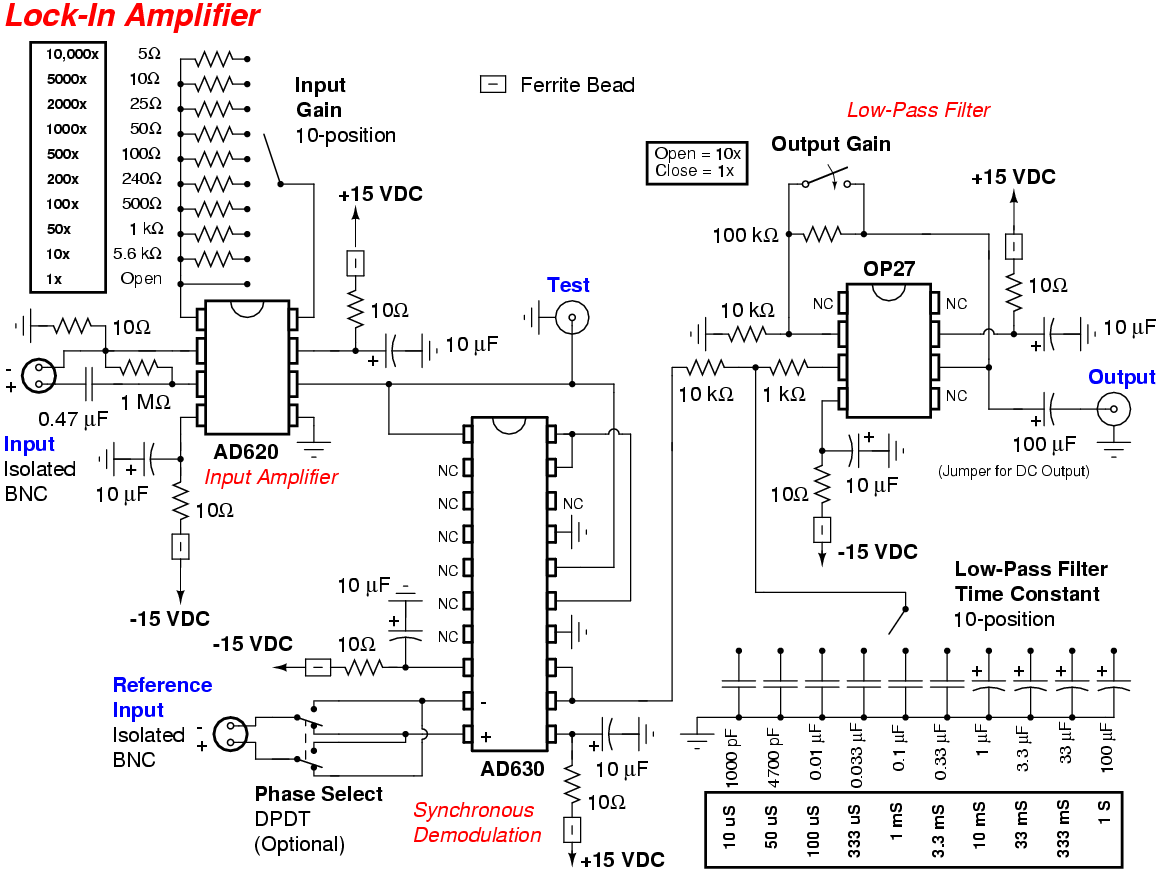
The lock-in amplifier is basically a synchronous demodulator followed by a low-pass filter. An important measure of performance in a lock-in amplifier is the dynamic range of its demodulator. With a properly designed lock-in amplifier, it is possible to extract a target signal from a noise signal approximately 100,000 times larger; which is a dynamic range of 100 dB.
Synchronous demodulation is based around the fact that 1 + (-1) = 0. What this means is, the synchronous receiver multiplies the incoming signal (using op-amp gain) by either +1 or -1 in sync with a some reference signal. Uncorrelated noise, or any other interfering signals, will average out to "zero." The "target" signal, riding on the reference signal, will not average to zero and can emerge from noise which is 100,000 times larger. For those who may not understand the significance of this, think of it as being able to listen to a person talk while they are standing next to a jet engine.
You can see why the amateur espionage enthusiast should have a lock-in amplifier in their toolbox. Things like "laser bounce listeners" really come to life when you modulate the illuminating laser with a reference signal, then extract the target signal using lock-in amplification. The key is to use a reference signal about 10 times greater than the target audio signals. For recovering speech up to around 3 kHz, you might try a reference signal based around a 32,768 Hz clock crystal source. The final target intelligence is then recovered using a sharp low-pass filter to attenuate any uncorrelated disturbances, like noise, while passing the target audio signals.

The lock-in amplifier project shown here comes from a technical paper entitled "A Simple Low-Cost Lock-In Amplifier for the Laboratory" by Sandip Sengupta, Jessica Farnham, and James Whitten at the Department of Chemistry and Center for Advanced Materials at the University of Massachusetts - Lowell. Their paper goes into much more detail on the construction and operation of this particular lock-in amplifier design, so it won't be covered here. A copy of the paper will be included on our website.
This lock-in amplifier will be based around an Analog Devices AD630 balanced modulator/demodulator. The AD630 has the ability to use it's internally-matched precision op-amps for lock-in amplification. An Analog Devices AD620 low-cost, low-power instrumentation amplifier will be used for the signal input amplifier because it has a larger signal bandwidth, instead of the Burr-Brown INA114 in the U. Mass paper. An OP27 low-noise precision op-amp will be used for the output low-pass filter. The AD620's gain will be selectable via a panel-mount 10-position rotary switch, and the output low-pass filter's time constant will also be selectable via a 10-position rotary switch.
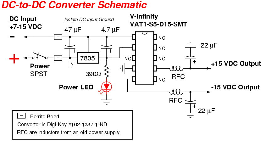
Isolated BNC connectors will be used for the input and reference signals, and a simple DC-to-DC converter will supply the +/- 15 volt power lines for the op-amps and AD630.
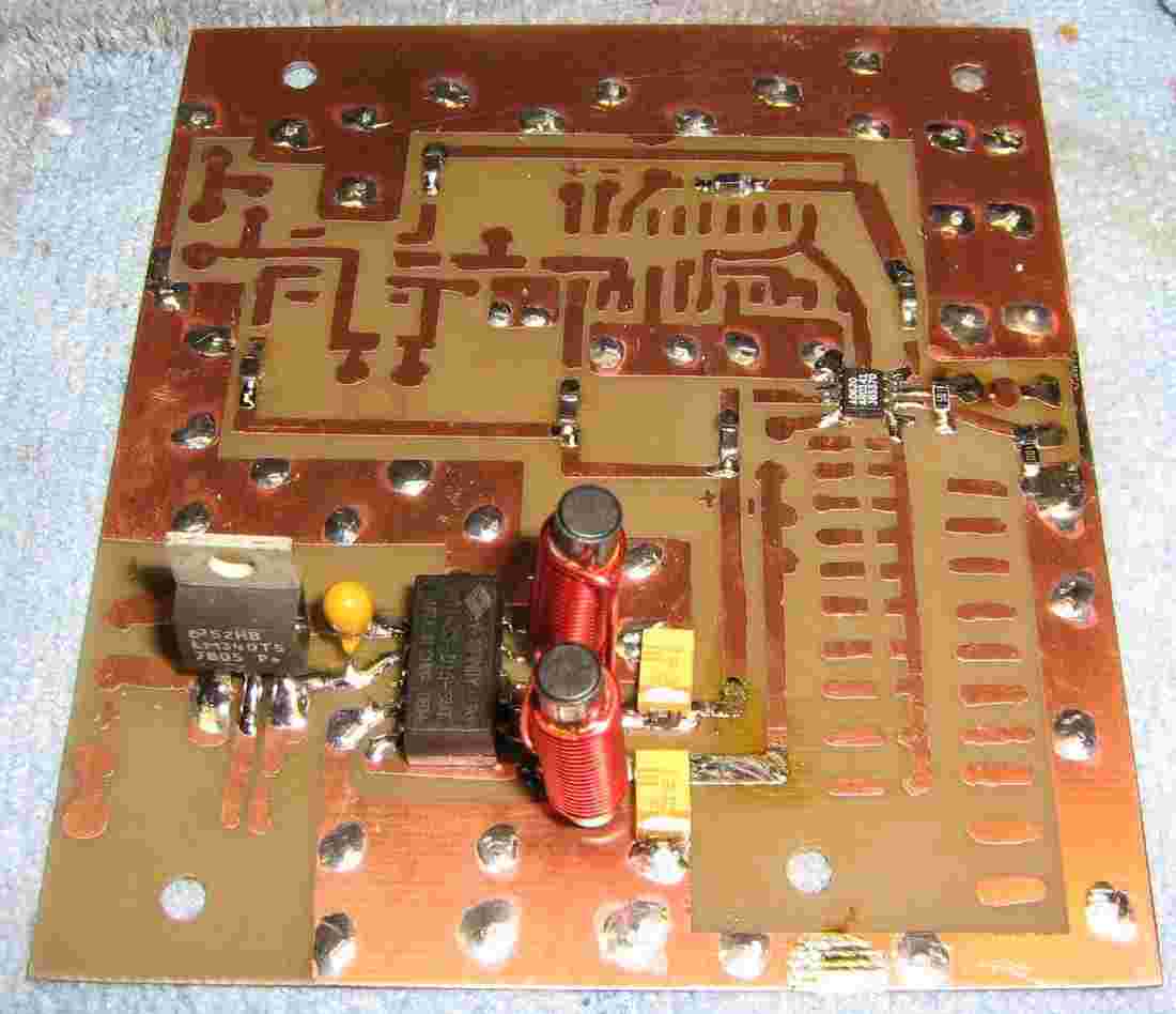
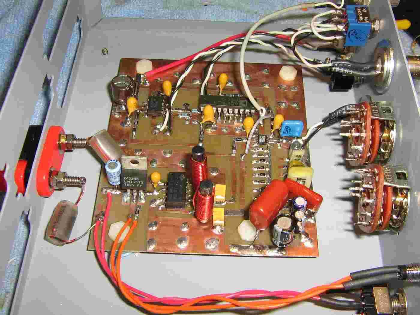
Overview of the lock-in amplifier's handmade printed circuit board.
The V-Infinity VAT1-S5-D15-SMT voltage converter (Digi-Key Part Number 102-1387-1-ND) is on the left, fed via an isolated 7805 voltage regulator. The DC-to-DC converter is setup to use an isolated ground to help prevent any ground loops.
The output of the VAT1-S5-D15-SMT is low-pass filtered using inductors salvaged from old computer power supplies and 22 µF tantalum capacitors. Be sure to note the capacitor's polarity, as the "positive" end is marked on a tantalum capacitor.
Note the use of a large ground plane and lots of ground vias. Ground loops can be a problem in high-gain precision circuits so you'll want to try and minimize them.
This project is still a "work in progress," so it will look a little rough. The overall concepts should still be applicable.
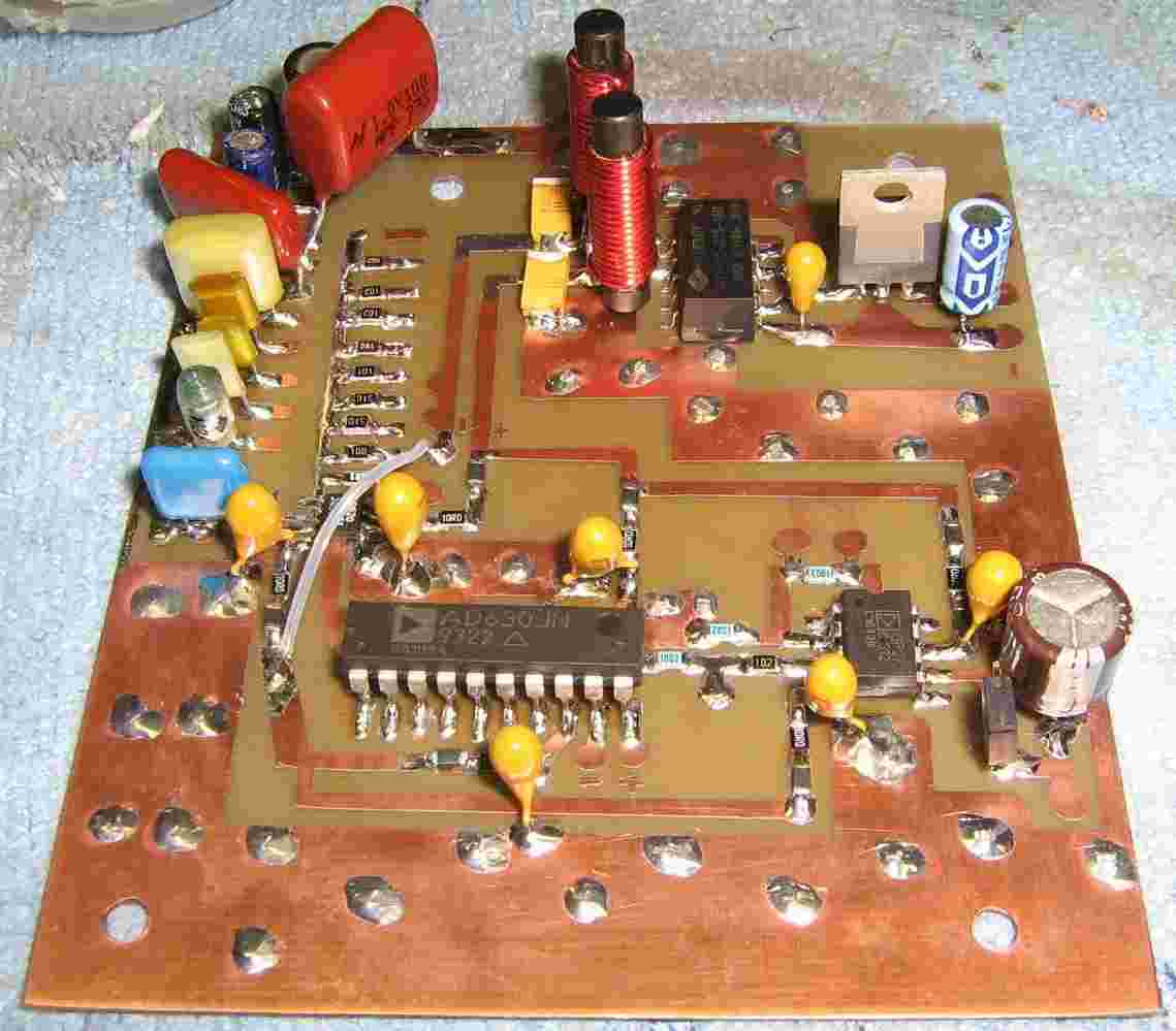
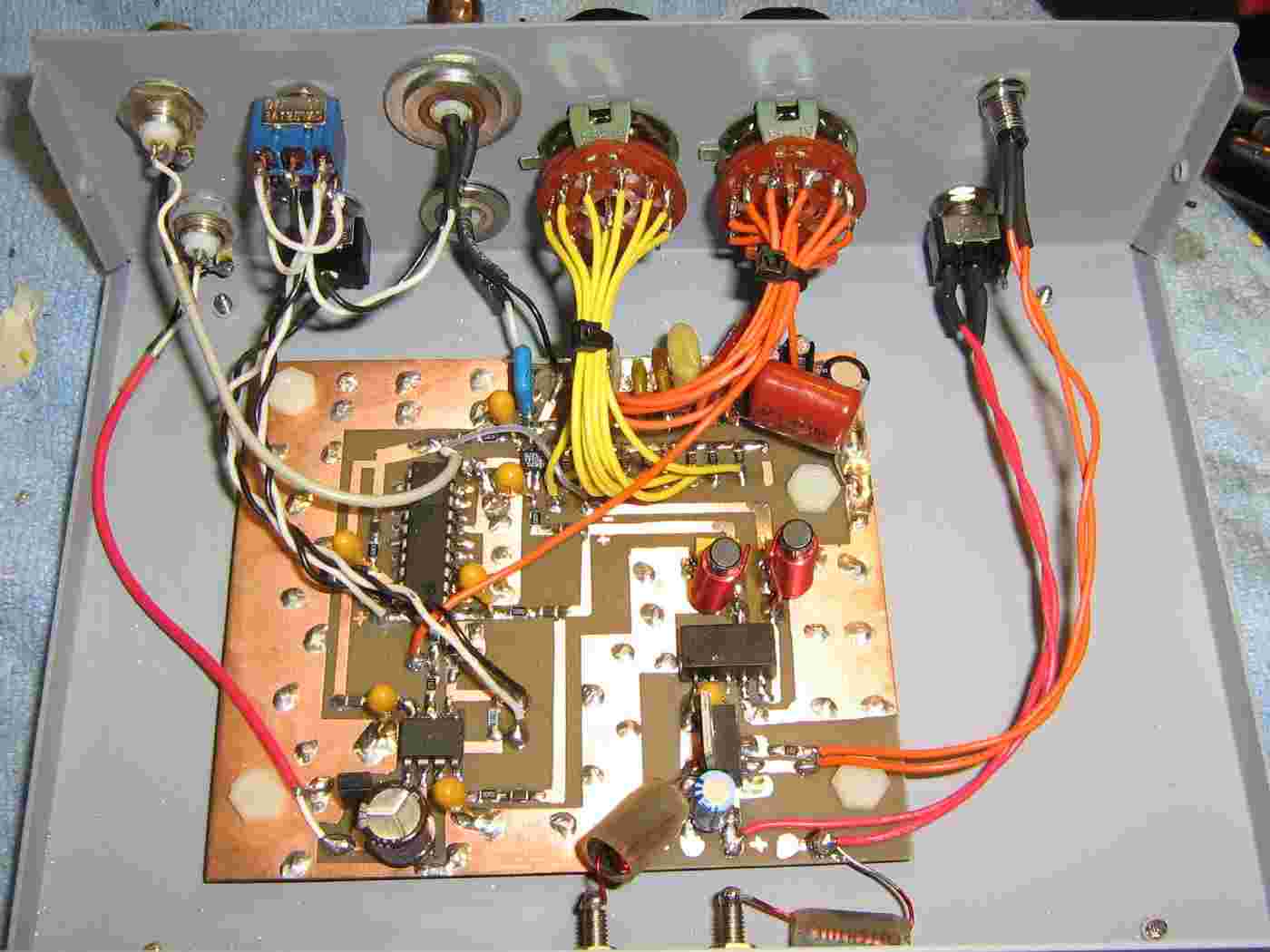
Completed lock-in amplifier circuit board.
The row of capacitors along the left are switched in-and-out for altering the time constant (cut-off frequency) of the output low-pass filter.
Next to them are the gain set resistors for the AD620 (Digi-Key Part Number AD620BNZ-ND [DIP]) input op-amp.
The AD630J (Digi-Key Part Number AD630JNZ-ND [DIP]) is in the middle.
The output of the OP27 op-amp (Digi-Key Part Number OP27GPZ-ND [DIP]) has a selectable jumper on it to allow for raw DC output, if needed. Otherwise, there is a series 100 µF capacitor.
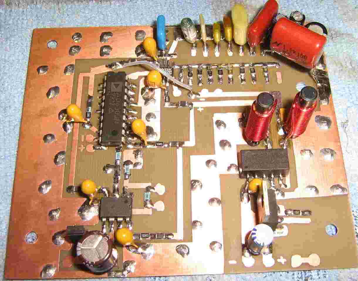
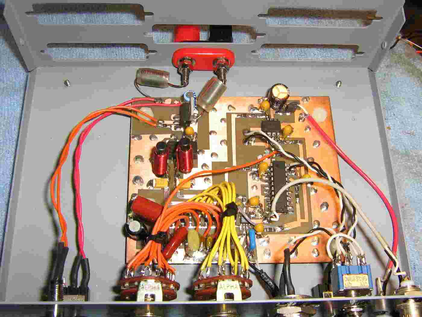
Completed lock-in amplifier circuit board. Alternate view.
Note the isolated incoming power lines on the lower-right.
Commercial lock-in amplifiers often have an adjustment to control the phase of the reference signal. This allows it to completely track the incoming signal, even if the reference signal phase is unknown.
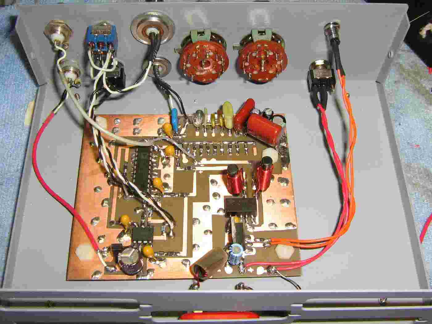
Starting to mount the lock-in amplifier circuit board and panel-mount components.
The case is from an old printer switch box. The circuit board itself is mounted on rubber grommets with nylon hardware to minimize ground loops and prevent the circuit board from picking up microphonic vibrations.
Note that the incoming and reference signals use isolated BNC connectors. This is also to help minimize ground loops. The test and output signals use standard panel-mount BNC connectors.
Two panel-mount 10-position switches allow for selecting the incoming gain and output low-pass filter time constants.
A DPDT switch allows you to flip the AD630's incoming reference signal between the "+" and "-" comparator op-amp inputs. This option is not necessary, but could be handy.
Alternate view.
Unregulated DC input comes in via the banana jacks on the left.
Try to use polyfilm capacitors in the low-pass filter time constant section.
Completed wiring top view.
Power switch and LED are on the right.
Completed wiring alternate view.
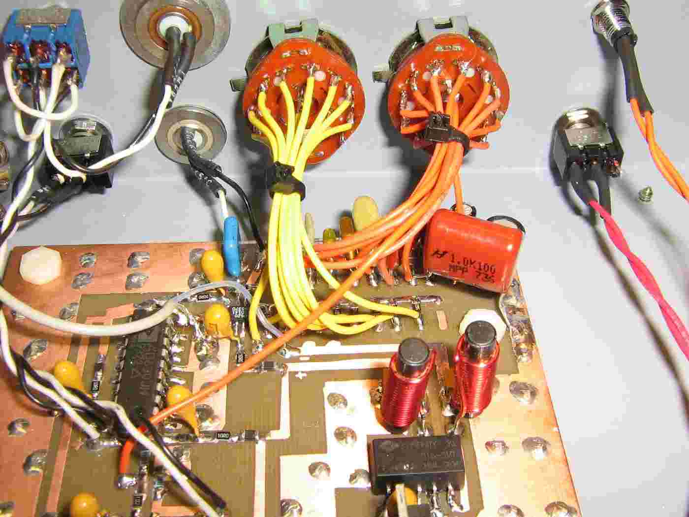
Closeup of the selector switch wiring.
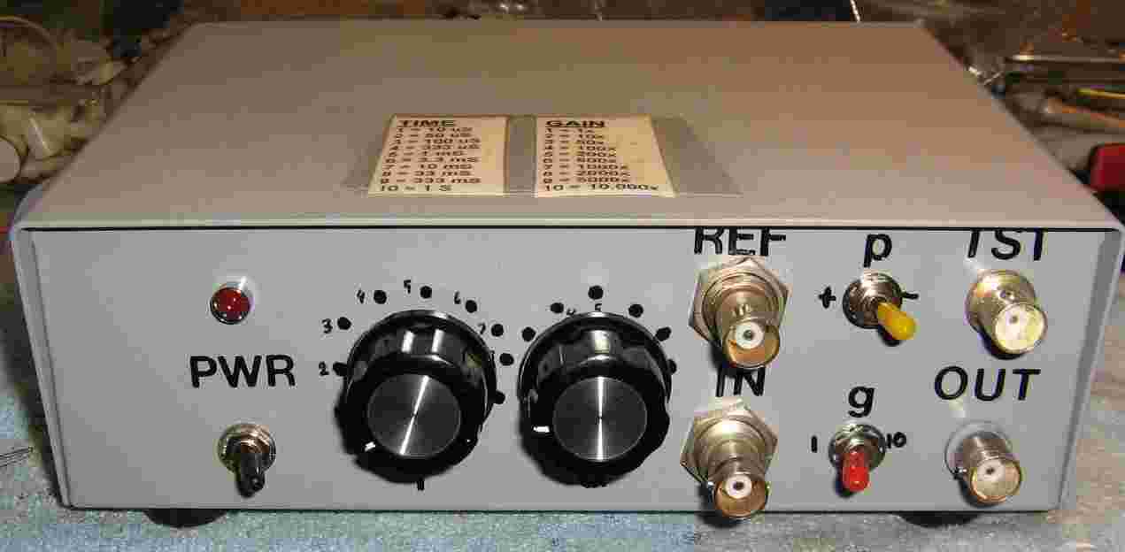
Front-panel overview.
PWR is the power switch and LED, REF is the reference signal input, IN is for the input signal, OUT is the low-pass filtered output, TST is a sample of the amplified input signal, P is the reference signal phase select switch, and G is the output op-amp's gain select switch, which is either 1 or 10.
The 10-position switch on the left selects the time constant and the one next to it is the gain select switch.
The top label for the rotary switch positions:
TIME               GAIN
1 = 10 µS          1 = 1x
2 = 50 µS          2 = 10x
3 = 100 µS         3 = 50x
4 = 333 µS         4 = 100x
5 = 1 mS           5 = 200x
6 = 3.3 mS         6 = 500x
7 = 10 mS          7 = 1,000x
8 = 33 mS          8 = 2,000x
9 = 333 mS         9 = 5,000x
10 = 1 S           10 = 10,000x